NCP167AMX330TBG Ultra-Low Noise, High PSRR LDO Regulator
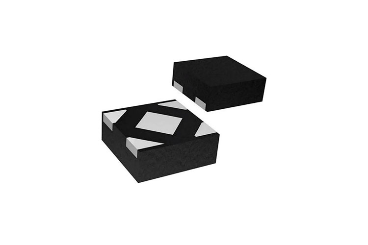
The NCP167AMX330TBG is a linear regulator capable of supplying 700 mA output current. Designed to meet the requirements of RF and analog circuits, the NCP167 AMX330TBG device provides low noise, high PSRR, low quiescent current, and very good load/line transients. The NCP167AMX330TBG is designed to work with a 1F input and a 1F output ceramic capacitor. It is available in an XDFN4 package with 1mmx1mmx0.4mm dimensions.
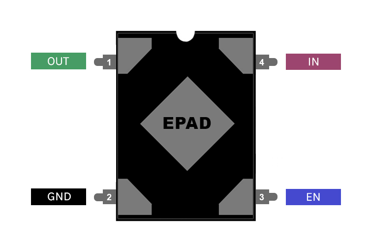
NCP167AMX330TBG Pinout Configuration
|
Pin Number |
Pin Name |
Description |
|
1 |
OUT |
Regulated output |
|
2 |
GND |
Common ground connection |
|
3 |
EN |
Chip enable |
|
4 |
IN |
Input voltage supply pin |
Features
- Operating Input Voltage Range: 1.9 V to 5.5 V
- Available in Fixed Voltage Option: 1.8 V to 5.2 V
- ±2% Accuracy Overload/Temperature
- Ultra-Low Quiescent Current Typ. 12 µA
- Standby Current: Typ. 0.1 µA
- Very Low Dropout: 210 mV at 700 mA
- Ultra-High PSRR: Typ. 85 dB at 20 mA, f = 1 kHz
- Ultra-Low Noise: 8.5 µVRMS
- Stable with a 1 µF Small Case Size Ceramic Capacitors
- These Devices are Pb−Free, Halogen Free/BFR Free and are RoHS Compliant
Absolute Maximum Ratings
|
Rating |
Symbol |
Value |
Unit |
|
Input Voltage |
Vin |
−0.3 V to 6 |
V |
|
Output Voltage |
VOUT |
−0.3 to VIN + 0.3, max. 6 V |
V |
|
Chip Enable Input |
VCE |
−0.3 to VIN + 0.3, max. 6 V |
V |
|
Output Short Circuit Duration |
tSC |
unlimited |
s |
|
Junction Temperature |
TJ |
150 |
°C |
|
Temperature |
TSTG |
-55 to 150 |
℃ |
|
ESD Capability, Human Body Model |
ESD HBM |
2000 |
V |
|
ESD Capability, Machine Model |
ESD MM |
200 |
V |
Other LDOs
AP2112, MIC5205, RT9193, MCP1702, MCI5219
Note: Complete technical details can be found in the NCP167AMX330TBG datasheet at this page’s end.
How To Use NCP167AMX330TBG LDO?
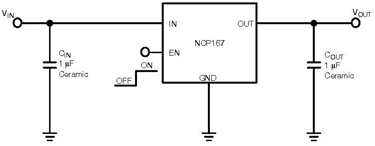
The schematics below show the typical application diagram of an NCP167AMX330TBG LDO. As mentioned earlier, it only requires a very minimal number of components, which includes the input and output filter capacitors.
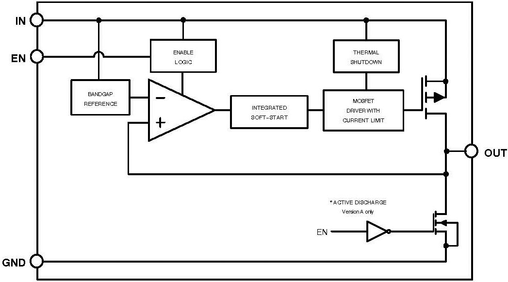
Functional Block Diagram
Applications
- Battery−powered Equipment
- Wireless LAN Devices
- Smartphones, Tablets
- Cameras, DVRs, STB, and Camcorders
DC Characteristics
|
Parameter |
Test Conditions |
Symbol |
Min |
Тур |
Max |
Unit |
|
|
Operating Input Voltage |
|
VIN |
1.9 |
|
5.5 |
V |
|
|
Output Voltage Accuracy (Note 5) |
VIN = VOUT(NOM) + 1 V to 5.5 V 0 mA ≤lOUT ≤ 700 mA |
VOUT |
-2 |
|
2 |
% |
|
|
Line Regulation |
VOUT(NOM) + 1 V≤ VIN ≤ 5.5 V |
LineReg |
|
0.02 |
|
% /V |
|
|
Load Regulation |
lOUT = 1 mA to 700 mA |
|
|
0.002 |
|
%/mA |
|
|
Dropout Voltage (Note 6) |
lOUT = 700 mA |
VOUT(NOM) = 1.8 V |
|
|
315 |
450 |
mV |
|
VOUT(NOM) = 3.3 V |
VDO |
|
190 |
290 |
|||
|
Output Current Limit |
VOUT = 90% VOUT(NOM) |
ICL |
800 |
1000 |
|
mA |
|
|
Short Circuit Current |
VOUT = 0 V |
Isc |
|
1050 |
|
||
|
Quiescent Current |
lOUT = 0 MA |
lQ |
|
9.7 |
18 |
μA |
|
|
Shutdown Current |
VEN ≤ 0.4 V, VIN = 4.8 V |
IDIS |
|
0.01 |
1 |
μA |
|
|
EN Pin Threshold Voltage |
EN Input Voltage "H" |
VENH |
1.2 |
|
|
V |
|
|
EN Input Voltage "L" |
VENL |
|
|
0.4 |
|||
|
EN Pull Down Current |
VEN = 4.8 V |
IEN |
|
0.2 |
0.5 |
μA |
|
|
Turn-On Time |
COUT 1 μF, From assertion of VEN to = VOUT = 95% VOUT(NOM) |
|
|
120 |
|
μs |
|
|
Power Supply Rejection Ratio |
VOUT(NOM) = 3.3 V, lOUT = 20 mA |
f = 100 Hz |
PSRR |
|
83 |
|
dB |
|
f = 1 kHz |
|
85 |
|
||||
|
f = 10 kHz |
|
80 |
|
||||
|
f = 100 kHz |
|
63 |
|
||||
|
Output Voltage Noise |
f = 10 Hz to 100 kHz |
lOUT = 20 mA |
VN |
|
8.5 |
|
μVRMS |
|
Thermal Shutdown Threshold |
Temperature rising |
TSDH |
|
160 |
|
°℃ |
|
|
Temperature falling |
TSDL |
|
140 |
|
°℃ |
||
|
Active output discharge resistance |
VEN < 0.4 V, Version A only |
RDIS |
|
280 |
|
Ω |
|
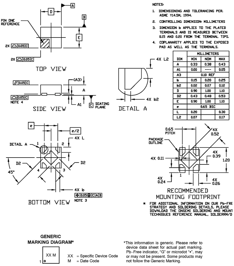
2D Model and Dimensions