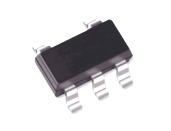
RT9193: Ultra-Fast LDO Regulator
RT9193 is an Ultra-Low Noise, Ultra-Fast CMOS LDO Regulator with power consumption less than 0.01μA in shutdown mode and has fast turn-on time less than 50μs. RT9193 has a low dropout voltage of 220 mV at 300mA and operating voltage range is from 2.5V to 5.5V, with an output voltage between 1.5V to 5V.
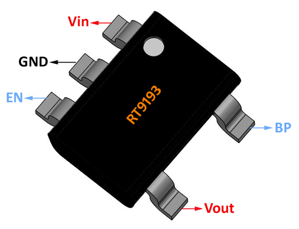
Pin Configuration
|
Pin No. |
Pin Name |
Description |
|
1 |
Vin |
Power Input Voltage |
|
2 |
GND |
Ground |
|
3 |
EN |
Chip Enable (Active High). This pin is high impedance. Connect a pull low 100kΩ Resistor to GND when the control signal is floating. |
|
4 |
BP |
Reference Noise Bypass. For lowest noise performance, connect a 22nF Capacitor between the BP and GND pins. |
|
5 |
Vout |
Output Voltage |
Features
- Input Supply Voltage: 2.5V to 5.5V
- Continuous Output Current: 300 mA
- Drop-out Voltage: 220 mV at 300 mA
- Output Voltage: 1.5V to 5V
- Standby Current: 0.01 µA
- Turn-on Time: 50 µs
- Available in SC-70-5, SOT-23-5, TSOT-23-5, WDFN-6L 2x2 and MSOP-8 packages.
Note: The Complete Technical Details can be found at the RT9193 datasheet given at the end of this page.
Equivalent for RT9193: RT9199, S-1135, NCP4635
Alternative LDO Regulators: AMS1117, MIC5225, XC6206
RT9193 Introduction
RT9193 is specially designed for portable RF and wireless applications with demanding performance and space requirements by RICHTEK. Output noise is further reduced by bypass pin. Functional block diagram of RT9193 is shown below. Main components of this regulator are the Reference voltage, Error amplifier, and Pass element (field-effect transistor). Resistor connected to positive pin are used for required output voltage.
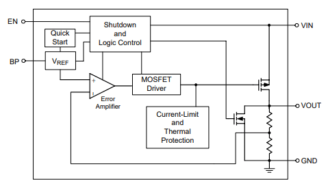
Because of its very low standby current and fast turn-on time, RT9193 is mostly used in CDMA/GSM Cellular Handsets and Portable Information Appliances.
How to Use RT9193
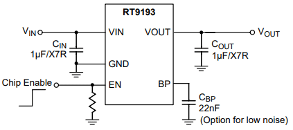
RT9193 is a 5-pin Low drop-out voltage regulator. In RT9193 regulator an extra bypass pin is introduced for further output noise reduction. This pin is connected to ground through an optional 22nf capacitor. Vin pin is connected to input power supply and a 1µf ceramic capacitor is used for input noise cancellation. Regulated voltage is obtained from Vout pin. Enable pin can be used turn on or off the regulator. Circuit diagram for RT9193 voltage regulator is shown below.
Applications
- CDMA/GSM Cellular Handsets
- Battery-Powered Equipment
- Laptop, Palmtops, Notebook Computers
- Hand-Held Instruments
- PCMCIA Cards
- Portable Information Appliances
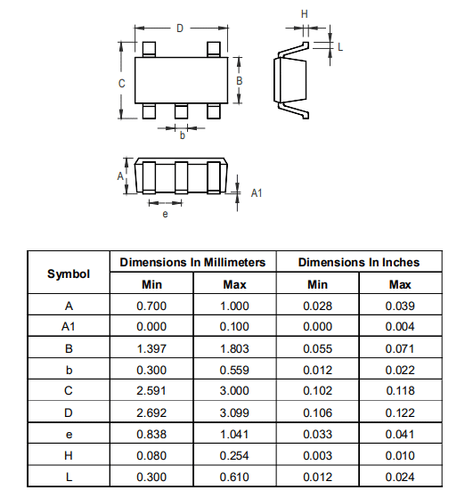
2D-Model (SOT-23-5)
