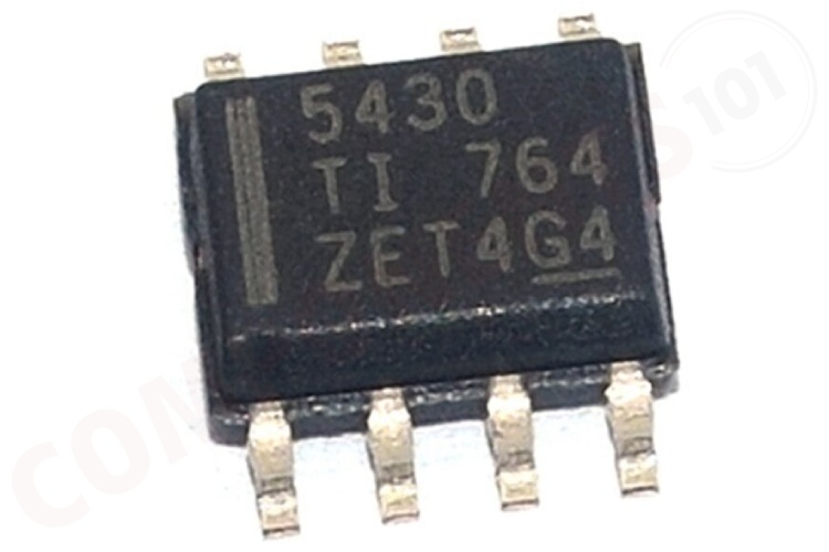
TPS5430 – 3A Step-Down Converter
The TPS5430 is a step-down converter from Texas Instruments, with integrated MOSFET and high current capability of up to 3A. With the low-resistance integrated MOSFET, the TPS5430 provides low conduction loss and higher efficiency. This regulator supports a wide input voltage range, usually from 5.5V to 36V. The IC offers safety features such as overcurrent limiting, overvoltage protection and thermal shutdown along with an enable pin for easy control. It also features an internally compensated feedback loop circuit which will help to reduce the external component count. The TPS5430 provides a fast transient response to changes in load conditions, which is very helpful for the circuit that needs stable outputs. The TPS5430 IC is available in a thermally enhanced, easy-to-use 8-pin SOIC PowerPAD package.
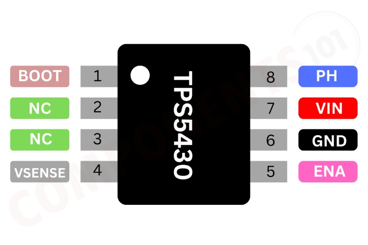
TPS5430 Pinout Configuration
Here are the pinout details for TPS5430.
| PIN NO | NAME | FUNCTION |
| 1 | BOOT | Boost capacitor for the high-side FET gate driver |
| 2,3 | NC | Not connected internally. |
| 4 | VSENSE | Feedback voltage for the regulator |
| 5 | ENA | Enable |
| 6 | GND | Ground. |
| 7 | VIN | Input supply voltage. |
| 8 | PH | Source of the high side power MOSFET. |
Features of TPS5430
The TPS5430 Switching regulator has the following key features:
- Wide input voltage range: – TPS5430: 5.5V to 36V
- Up to 3A continuous (4A peak) output current
- High efficiency up to 95% enabled by 100mΩ integrated MOSFET switch
- Wide output voltage range: adjustable down to 1.22V with 1.5% initial accuracy
- Internal compensation minimises external parts count
- Fixed 500kHz switching frequency for small filter size
- Improved line regulation and transient response by input voltage feedforward
- System protected by overcurrent limiting, overvoltage protection, and thermal shutdown
- –40°C to 125°C operating junction temperature range
- Available in small thermally enhanced 8-pin SO PowerPAD™ integrated circuit package
Manufacturers of TPS5430:
Texas Instruments manufactures the TPS5430. There are no alternative manufacturers for the same part number as of the date of writing this article.
TPS5430 Equivalents
If you are looking for pin-to-pin compatible equivalents for TPS5430 you can use TPS5431
TPS5430 Alternatives
If you are looking for an alternative for TPS5430 you can look at the other IC from these.
LM2596, XL6009, MC34063, MP9486, MP1584, TPS54231, LM2576, CS1411, LT1070, RT8059, NCP3170, LT1370, LT1765
Note: Complete technical details can be found in the TPS5430 datasheet at this page’s end.
TPS5430 Circuit Diagram
The following image shows a simple circuit diagram for TPS5430.
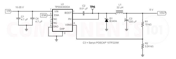
This above circuit is a typical application circuit of TPS5430. The circuit provides stable 5V out from a 10-35v input.
In this circuit, input is supplied to the VIN pin. The C1 and C4 capacitors filter the input voltage (VIN), reduce noise, and stabilise the input voltage. The EN pin is used to enable or disable the converter. When connected to a high voltage, the converter is enabled; when connected to a low voltage, it is disabled. Capacitor C2 is used as a boost capacitor for driving the high-side MOSFET driver. The inductor stores energy when the high-side MOSFET is on and releases it when the MOSFET is off. The diode provides a path for the inductor current when the high-side MOSFET is off, preventing it from flowing back into the MOSFET and causing damage. The output filter capacitor C3 smooths out the output voltage and reduces voltage ripple. R1 and R2 resistors form a voltage divider that sets the output voltage. The feedback pin of the TPS5430 reads the voltage from this resistor divider to regulate the output.
Troubleshooting Tips for TPS5430 Circuit
There is no output from the circuit. What could be the issue?
First, ensure that the power supply voltage and current are sufficient. Check the connections to the TPS5430. Properly connect the inductor. Make sure the EN pin is high.
TPS5430 IC is getting very hot even without load.?
Check the output pin of TPS5430 first. Check whether there is any chance of a short circuit and make sure the pad is connected to the ground. If the problem persists, try to change the TPS5430.
I'm experiencing a lot of ripples on the TPS5430 output. What might be causing this?
Make sure to use the appropriate filter capacitor at the input and output.
Things to Consider When Using TPS5430 in Your Design
Power Supply Recommendations
The TPS5430 is designed to operate from an input voltage supply range between 5.5 V and 36 V. The TPS5431 is designed to operate from an input voltage supply range between 5.5 V and 23 V. This input supply must remain within the input voltage supply range. If the input supply is located more than a few inches from the TPS543x converter bulk capacitance can be required in addition to the ceramic bypass capacitors. An electrolytic capacitor with a value of 100 μF is a typical choice.
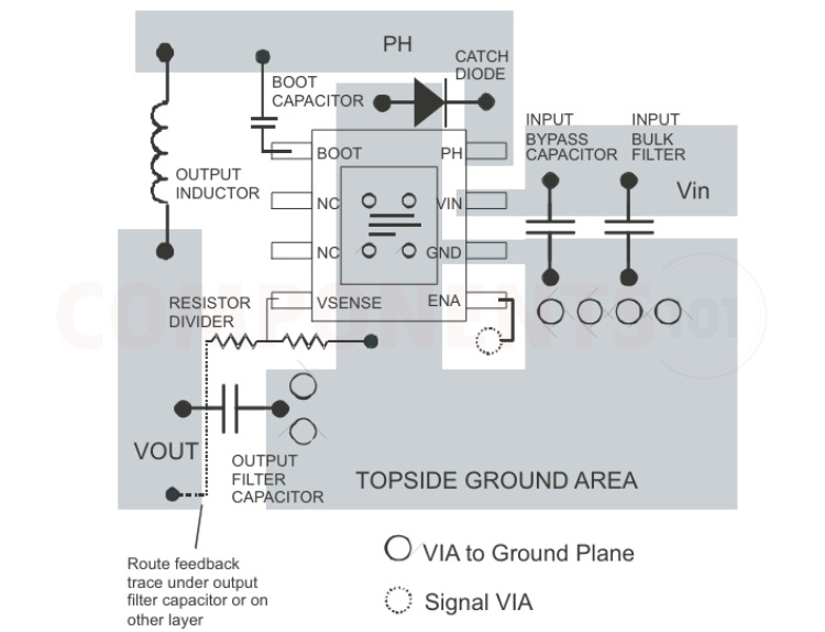
Layout Guidelines
Connect a low ESR ceramic bypass capacitor to the VIN pin. Care must be taken to minimise the loop area formed by the bypass capacitor connections, the VIN pin, and the TPS543x ground pin. The best way to do this is to extend the top-side ground area from under the device adjacent to the VIN trace and place the bypass capacitor as close as possible to the VIN pin. The minimum recommended bypass capacitance is 4.7 μF ceramic with an X5R or X7R dielectric. There must be a ground area on the top layer directly underneath the IC, with an exposed area for connection to the DAP. Use vias to connect this ground area to any internal ground planes. Use additional vias at the ground side of the input and output filter capacitors as well. The GND pin must be tied to the PCB ground by connecting it to the ground area under the device as shown below. The PH pin must be routed to the output inductor, catch diode and boot capacitor. Because the PH connection is the switching node, the inductor must be located very close to the PH pin and the area of the PCB conductor is minimised to prevent excessive capacitive coupling. The catch diode must also be placed close to the device to minimize the output current loop area. Connect the boot capacitor between the phase node and the BOOT pin as shown. Keep the boot capacitor close to the IC and minimize the conductor trace lengths. The component placements and connections shown work well, but other connection routings can also be effective. Connect the output filter capacitor(s) as shown between the VOUT trace and GND. It is important to keep the loop formed by the PH pin, Lout, Cout and GND as small as is practical. Connect the VOUT trace to the VSENSE pin using the resistor divider network to set the output voltage. Do not route this trace too close to the PH trace. Due to the size of the IC package and the device pin-out, the trace can need to be routed under the output capacitor. Alternatively, the routing can be done on an alternate layer if a trace under the output capacitor is not desired. If using the grounding scheme shown below, use via connection to a different layer to route to the ENA pin.
Applications of TPS5430
- Set-top box
- DVD Players
- LCD displays
- Industrial and car audio power supplies
- Battery chargers
- High-power LED supply
- 12V and 24V distributed power systems
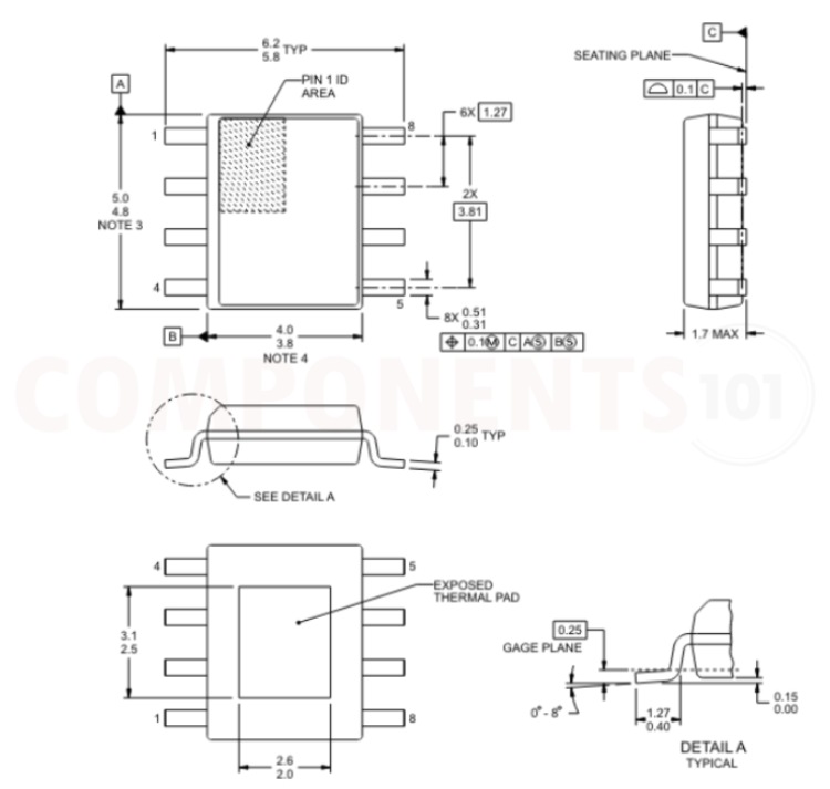
2D Model and Dimensions of TPS543
Here you can find the mechanical drawings of TPS5430 along with its dimensions. The dimensions can be used to create custom footprints of the IC and be used for PCB or CAD modelling.