CS51411 Buck Regulator
CS51411 is a 1.5A, 260 kHz and 520 kHz, Low Voltage Buck Regulator with External Bias or Synchronization Capability. The input voltage range for CS51411 is from 4.5V to 40V. The CS51411 is functionally pin−compatible with the LT1375.
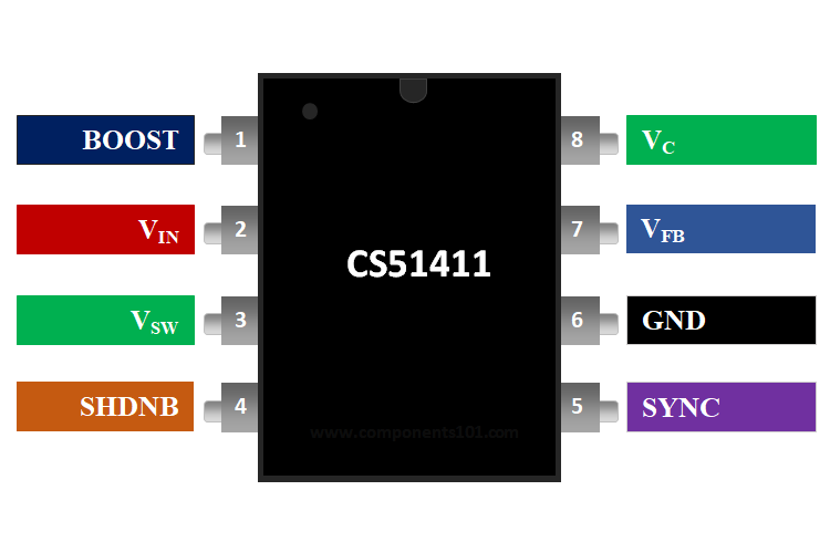
Pin Configuration of CS51411
|
Pin Number |
Pin Name |
Description |
|
1 |
BOOST |
The BOOST pin provides additional drive voltage to the on−chip NPN power transistor |
|
2 |
VIN |
Power Supply Pin |
|
3 |
VSW |
This pin is connected to the emitter of the on−chip NPN power transistor and serves as the switch output to the inductor |
|
4 |
SHDNB |
Shutdown_bar input. An active-low logical input pin. |
|
5 |
SYNC |
The synchronization input pin. |
|
6 |
GND |
Ground Pin |
|
7 |
VFB |
The FB pin provides input to the inverting input of the error amplifier |
|
8 |
VC |
The VC pin provides a connection point to the output of the error Amplifier and input to the PWM comparator. |
Features & Specifications of CS51411
- Input Voltage Min: 4.5V
- Input Voltage Max: 40V
- Output Voltage Range: 1.27V to 40V
- Frequency adj./ ext.clock min: 305 kHz
- Frequency adj./ ext.clock max: 470 kHz
- Quiescent current max: 6250 µA
- Inductor size: 15.00 µH
- BOOST pin for Bootstrapped Operation
- Maximized Efficiency
- Synchronization Function
- Parallel Supply Operation or Noise Minimization
- Shutdown Lead Provides Power-Down Option
- Available in 8-Pin SOIC and 18-Pin DFN Packages
Note: Complete Technical Details can be found at the CS51411 datasheet given at the end of this page.
CS51411 Equivalent
CS51412, CS51413, CS51414
Alternative DC-DC Controllers
Where to use CS51411 IC
The CS51411 buck regulator provides leading-edge technology, a high level of integration and high operating frequencies allowing the layout of a switch-mode power supply in a very small board area. CS51411 uses the V2™ control architecture to provide an unmatched transient response, the best overall regulation and the simplest loop compensation for today’s high−speed logic. Protection circuitry includes thermal shutdown, cycle−by−cycle current limiting, and frequency fold back.
The input voltage for the IC is from 4.5V to 40V and the output voltage can be varied from -1.27V to 40V. The CS51411 is pin−compatible with the LT1375.So if you looking for a buck voltage regulator with a wide input/output voltage range then CS51411 might be of interest to you.
How to use CS51411 IC
An Application diagram for 4.5 V − 16 V to 3.3 V @ 1.0 A Converter from CS51411 datasheet is shown below:
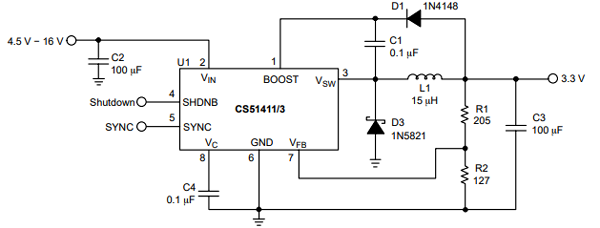
Input voltage is applied to the VIN pin of IC. A 100µF capacitor is connected to the input pin through the ground to cut down the ripple current. The VSW pin is connected to 15µH inductor. Lower inductor values are chosen to reduce the physical size of the inductor. Higher value inductors can be used to cuts down the ripple current, core losses, and allow more output current.
Applications of CS51411
- Blood Gas Analysers: Portable
- Cable Solutions
- HMIs (Human Machine Interfaces)
- Telecommunications
- Portable Devices
- Consumer & Computing
- Test & Measurement
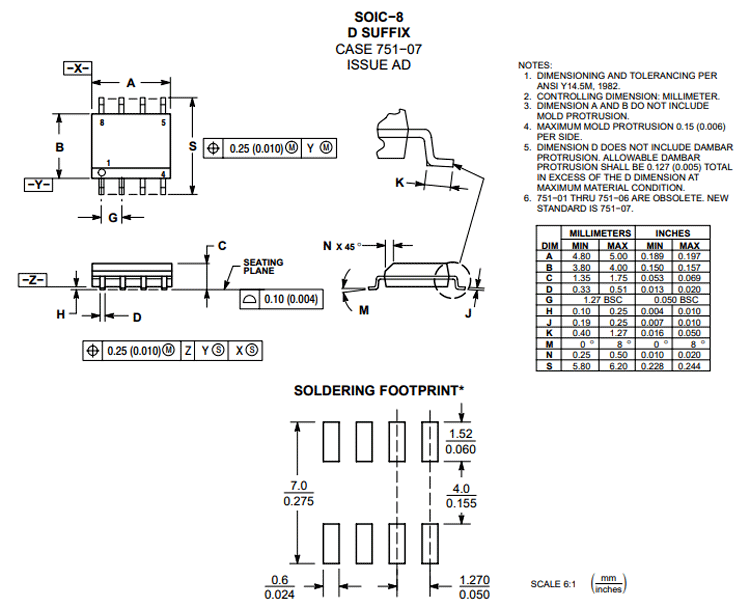
2D Model of CS51411
Dimensions for CS51411 IC is given below. These dimensions are for the SOIC package. If you are using different package IC please refer to the CS51411 datasheet.