LT1070 – High Power Buck, Boost and Flyback Switching Regulator
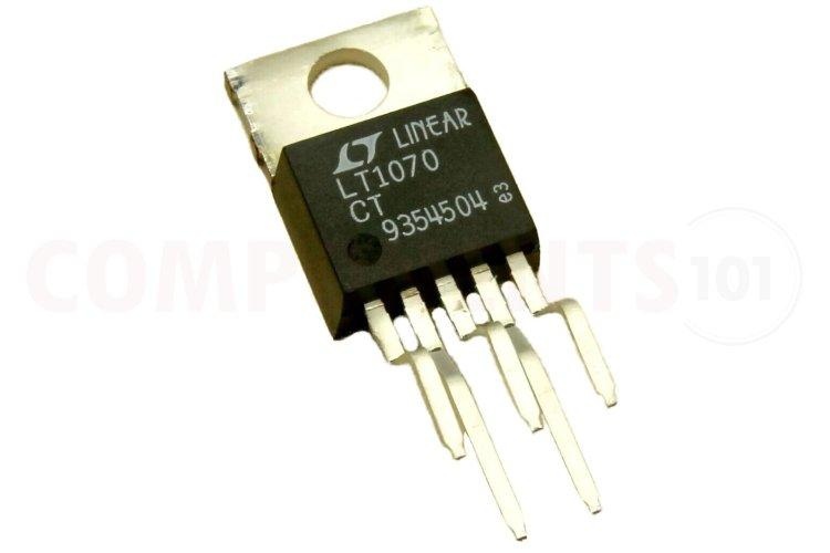
The LT1070 is a low-cost, high-power, high efficiency switching regulator. The LT1070 comes in all standard switching configurations including buck, boost, flyback, forward, inverting and “Cuk”. It can be operated with supply voltages from 3V to 60V and draws only 6mA quiescent current. This IC can deliver up to 100W power with no external power devices. It provides excellent AC and DC load and line regulation by utilizing current mode switching techniques. The LT1070 has many unique features. The Adaptive Antisat Switch Drive feature helps the circuit maintain high efficiency across a wide range of load currents. It adjusts the switching behavior to prevent saturation, which can improve efficiency and performance in varying load conditions. Externally Activated Shutdown Mode allows the user to manually put the device into a low-power state when it's not needed, this will reduce the overall supply current to 50µA during standby. The LT1070 can generate isolated outputs without needing additional components like optocouplers or extra transformer windings. The IC comes in a standard 5-pin T0-220 power package.
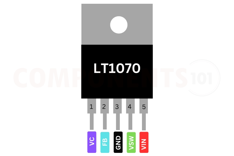
LT1070 Pinout Configuration
Here are the pinout details for MCP3301.
| Pin Number | Name | Function |
| 1 | VC | Voltage compensation |
| 2 | FB | Feed back |
| 3 | GND | Ground |
| 4 | VSW | Output /switching mode |
| 5 | VIN | Supply input |
Features of LT1070
LT1070 Switching regulator has the following key features:
- Wide Input Voltage Range: 3V to 60V
- Low Quiescent Current: 6mA
- Internal 5A Switch (2.5A for LT1071)
- Very Few External Parts Required
- Self-Protected Against Overloads
- Operates in Nearly All Switching Topologies
- Shutdown Mode Draws Only 50µA Supply Current
- Flyback Regulated Mode Has Fully Floating Outputs
- Comes in Standard 5-Pin TO-220 Package
- Can be Externally Synchronized
Manufacturers of LT1070:
The LT1070 is manufactured by Analog Devices (Formerly by Linear Technology, acquired by Analog Devices). There are no alternative manufacturers for the same part number as of the date of writing this article.
LT1070 Equivalents
If you are looking for an equivalent replacement for LT1070, you can use LT1071 from the same family. You could also use LT1070HV or LT1071HV, which have a higher input voltage range.
LT1070 Alternatives
If you are looking for an alternative for LT1070 you can look at the other IC from these.
LM2596, XL6009, MC34063, MP9486, MP1584, TPS54231, LM2576, CS1411, TPS5430, NCP3170, RT8059, LT1765, LT1370
Note: Complete technical details can be found in the LT1070 datasheet at this page’s end.
LT1070 Circuit Diagram
The following image shows a simple circuit diagram for LT1070.
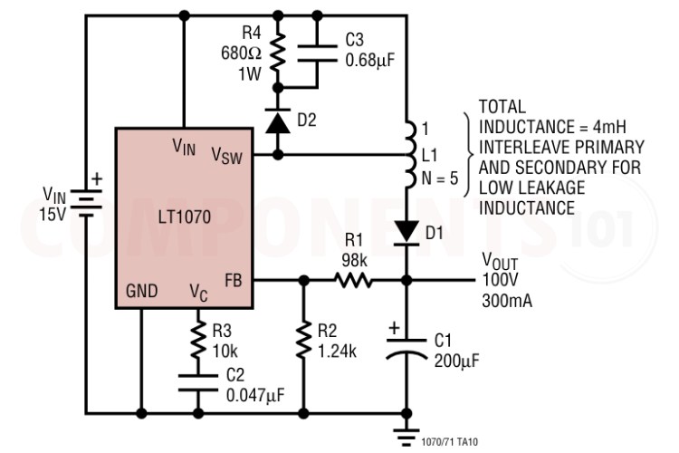
This circuit is designed to convert an input voltage of 15V to an output voltage of 100V at a current of 300mA. In this circuit 15V input is supplied to the VIN pin, the switching pin connected to the inductor L1. The feedback pin monitors the output voltage through the voltage divider. The inductor works with the LT1070 to store energy when the switch inside the LT1070 is on and releases energy to boost the voltage when the switch is off. Diode D1 rectifies the boosted voltage from the inductor and allows it to flow to the output capacitor C1. The capacitors C1, C2 and C3 are used to stabilize, filter and smooth the rectified output voltage.
The R1 and R2 resistors form a voltage divider network to provide feedback to the LT1070 to regulate the output voltage.
When power is applied, the LT1070 starts switching. The internal switch of the LT1070 (connected to the VSW pin) turns on and off, causing current to flow through L1. When the switch is on, current flows through the inductor L1, storing energy in its magnetic field. When the switch turns off, the magnetic field in L1 collapses, and the stored energy is released. This causes the voltage to rise significantly, which is then rectified by D1. The rectified high voltage is stored in the output capacitor C1, which smooths the output to provide a steady DC voltage of 100V.
The output voltage is sensed by the voltage divider network (R1 and R2) and fed back to the FB pin of the LT1070. The LT1070 adjusts its duty cycle to maintain the desired output voltage of 100V. R4, C3, and D2 form a snubber network that protects the internal switch of the LT1070 from voltage spikes generated when the inductor's magnetic field collapses.
LT1070 Troubleshooting Guide
My LT1070 (booster) is not providing any output. What could be the issue?
First, ensure that the power supply voltage and current are sufficient. Check the connections to the LT1070. Properly connect the inductor.
I'm experiencing varying output from the LT1070. What might be causing this?
Varying output can be due to noise in the circuit. Ensure that the input voltage is properly filtered. Verify that the ground connections are solid and check the filter capacitors.
The boost converter needs to start up properly or take too long to start. How can I troubleshoot this issue?
The possible causes of this issue are Insufficient input voltage or current at start-up and incorrect soft-start configuration. Excessive inrush current causes protection circuits to trip. To solve this, ensure the input power supply can provide sufficient voltage and current at start-up. Use inrush current limiting techniques, such as thermistors or controlled soft-start circuits.
Things to Consider When Using LT1070 in your Design:
When designing with the LT1070, here are some important considerations and design tips to keep in mind:
Power Supply Decoupling and Layout: Implement proper power supply decoupling with capacitors placed close to the LT1070 to provide stable voltage rails and reduce noise. While designing PCBs with LT1070, remember to place all components close to each other. Ensure the track widths are okay to handle the current and voltage ratings. Also, provide a proper ground plane in the PCB.
Temperature and Environmental Considerations: Consider the operating temperature range and environmental conditions in which the LT1070 will be used. Always use the heatsink for proper heat decapitation
Applications of LT1070
- Logic Supply 5V at 10A
- 5V Logic to ±15V Op Amp Supply
- Off-Line Converter Up to 200W
- Battery Upconverter
- Power Inverter (+ to –) or (– to +)
- Fully Floating Multiple Outputs
- For Lower Current Applications, See the LT1072
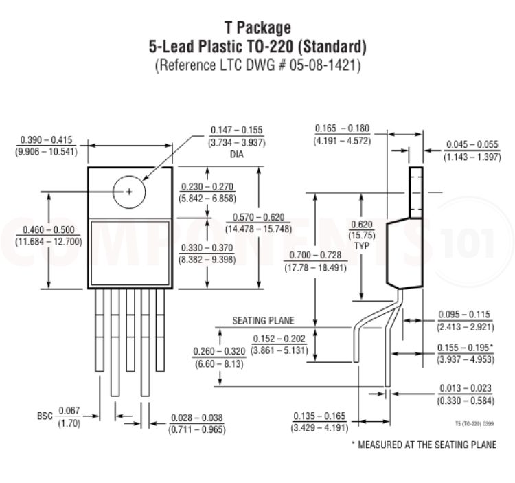
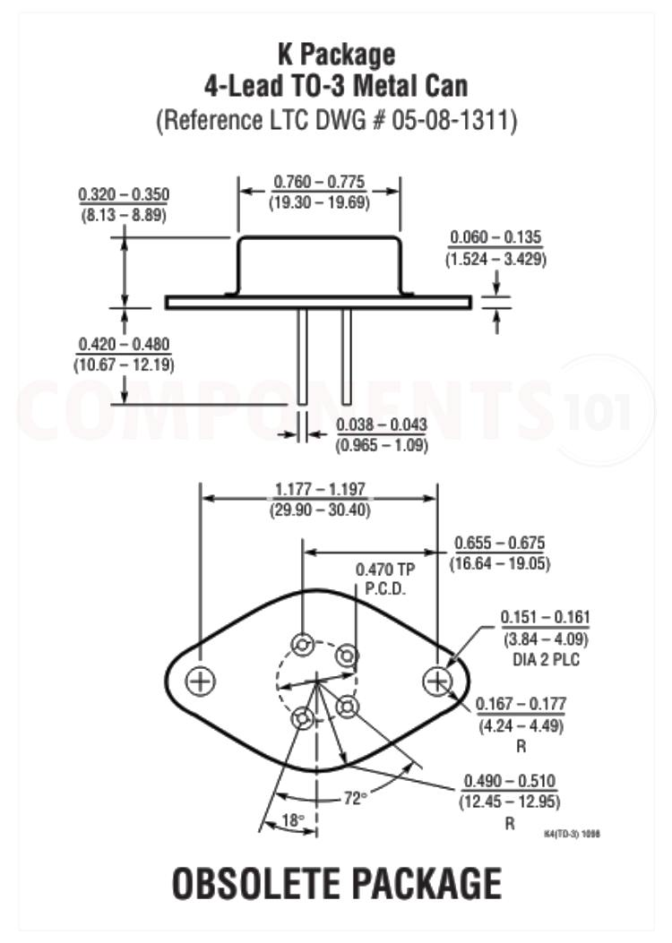
2D Model and Dimensions of LT1070
Here you can find the mechanical drawings of LT1070 along with its dimensions. The dimensions can be used to create custom footprints of the IC and be used for PCB or CAD modelling. The LT1070 was available in two packages (TO-220 and TO-3) in the past and at present only available in one package (TO-220).