MP9486 Step-Down Converter
The MP9486 is a high-voltage, step down converter from Monolithic Power Systems. It can deliver up to 1A of continues current. The MP9486 can handle a wide range of input voltage ranging from 4.5V to 100V. The integrated power MOSFET has a maximum current limit of 2.5A. The MP4986 features hysteric voltage mode control for very fast response. It also features a proprietary feedback control which minimizes the number of required external components. Other feature includes high switching frequency up to 1Mhz, thermal shutdown and short circuit protection. The low quiescent current of 170uA makes the MP9486 a better choice for battery powered application.
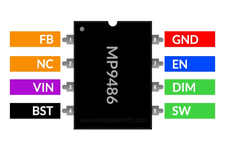
MP9486 Pinout Configuration
| Pin | Name | Description |
| 1 | FB | Feedback. FB is the input to the voltage hysteretic comparators. The average FB voltage is maintained at 200mV by loop regulation. |
| 2 | NC | No connection. |
| 3 | VIN | Input supply. VIN supplies power to all of the internal control circuitries, both BST regulators, and the high-side switch. A decoupling capacitor to ground must be placed close to VIN to minimize switching spikes. |
| 4 | BST | Bootstrap. BST is the positive power supply for the internal, floating, high-side MOSFET driver. Connect a bypass capacitor between BST and SW. |
| 5 | SW | Switch node. SW is the output from the high-side switch. A low forward voltage Schottky rectifier to ground is required. The rectifier must be placed close to SW to reduce switching spikes. |
| 6 | DIM | PWM dimming input. DIM is useful in LED driver applications. Pull DIM below the specified threshold for dimming off. Pull DIM above the specified threshold for dimming on. If the dimming function is not needed, such as in common buck applications, then connect DIM and EN together. |
| 7 | EN | Enable input. Pull EN below the specified threshold to shut down the MP9486. Pull EN above the specified threshold or leave EN floating to enable the MP9486. |
| 8 | GND | Ground. GND should be placed as close to the output capacitor as possible to avoid the high-current switch paths. Connect the exposed pad to GND plane for optimal thermal performance. |
Features
- Wide 4.5V to 100V Input Range
- Hysteretic Control: No Compensation
- Up to 1MHz Switching Frequency
- PWM Dimming Control Input for LED Application
- Short-Circuit Protection (SCP) with Integrated High-Side MOSFET
- 170μA Quiescent Current
- Thermal Shutdown
- Available in a SOIC-8 Package with an Exposed Pad
Other Popular Buck Converter ICs
LM2675, ADP2302, L7987L, TPS54331, NCP3170, RT8059, XL6009, TPS5430, MC34063, LM2596
Note: Complete technical details can be found in the MP9486 datasheet at this page’s end.
MP9486 Schematic Diagram
Image below shows the typical schematic diagram for MP9486.
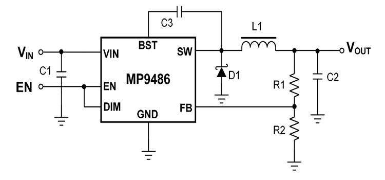
The circuit below is buck converter with an output voltage of 5V with a maximum current of 1A. The VIN can be anywhere from 8-95V DC. As you can see the required components are bare minimum, and include the input filter capacitors, boot strap capacitor, switching inductor, output rectifier diode, output filter capacitors and the resistor divider for voltage feedback. The output voltage (Vout) is set using the resistor divider built around the resistors R1 and R2. To archive good noise immunity and power loss, the recommended value for R2 is 5kOhms to 50kOhms. The value of R1 can be calculated using the following equation, where Vfb is 0.2v.
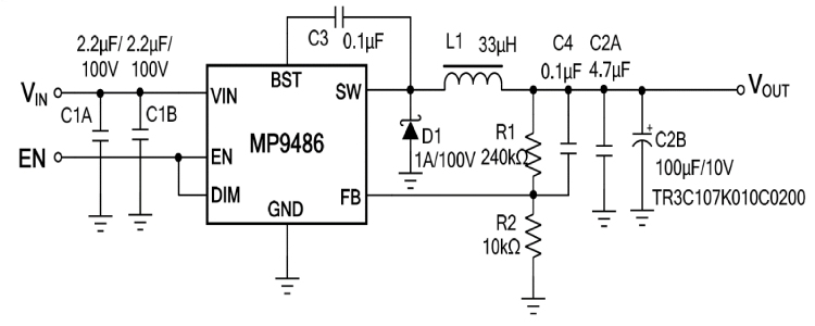
R1=(V_Out- V_Fb)/V_Fb ×R2
Applications
- Scooters, E-Bike Control Power Supplies
- Solar Energy Systems
- Automotive System Power
- Industrial Power Supplies
- High-Power LED Drivers
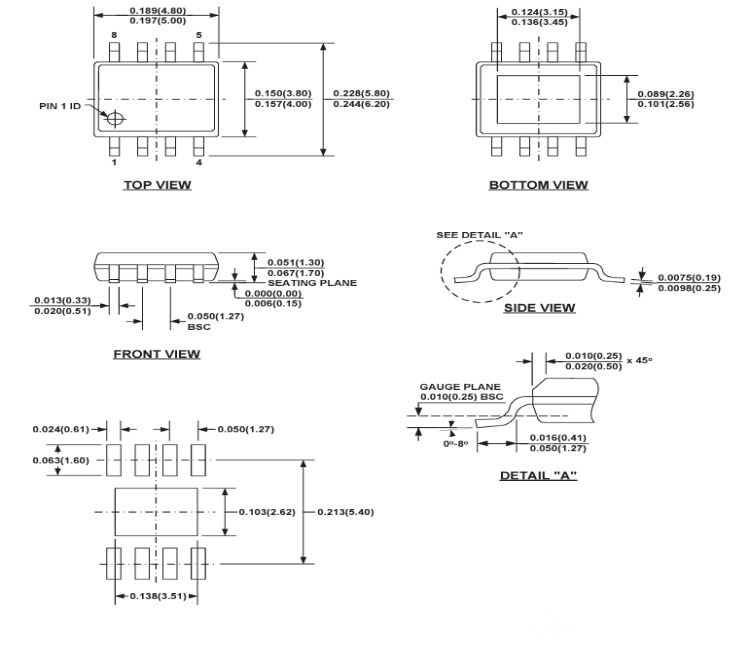
2D-Model and Dimensions
Below is the 2D CAD drawing of MP9486 along with its dimensions in inches (millimeters). The dimensions can be used to create custom footprints of the module and be used for PCB or CAD modelling.