TPS54231DR Step-Down Buck Converter IC 3.5 to 28V Input, 2A, 570kHz
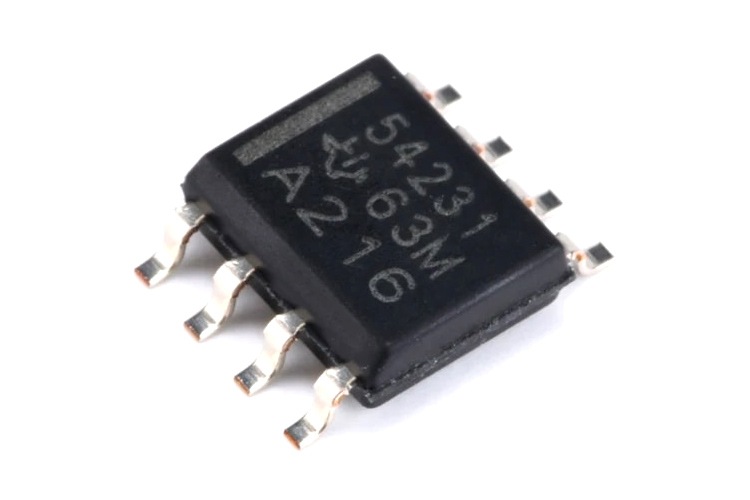
The TPS54231 is a 2A non-synchronous buck converter from Texas Instruments. The TPS54321DR has an integrated low RDS (on) high-side MOSFET, designed to enhance efficiency in various electronic applications. This device features a pulse-skipping Eco-mode for increased efficiency at light loads, ideal for battery-powered applications, thanks to its ultra-low 1-µA shutdown supply current. Current mode control with internal slope compensation simplifies external compensation calculations and reduces component count, allowing the use of ceramic output capacitors. It also includes a resistor divider for input Undervoltage lockout hysteresis, overvoltage transient protection to limit voltage overshoots, and a cycle-by-cycle current limit scheme with frequency foldback and thermal shutdown for overload protection. Encased in an 8-pin SOIC package optimized for thermal performance, the TPS54231 is a versatile choice for efficient power management in a compact footprint. Please note that the part numbers TPS54231D and TPS54231DR are both similar in working, the only difference is with their packaging quantity (SPQ), the TPS54231D has 75 units in a roll and the TPS54231DR has 2500 units in a roll.
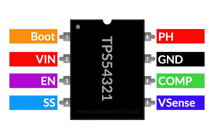
TPS54321 Pinout Configuration
| Pin Name | I/O | Description | |
| 1 | Boot | O | A 0.1-μF bootstrap capacitor is required between the BOOT and PH pins. If the voltage on this capacitor falls below the minimum requirement, the high-side MOSFET is forced to switch off until the capacitor is refreshed. |
| 2 | VIN | I | This pin is the 3.5- to 28-V input supply voltage |
| 3 | EN | I | This pin is the enable pin. To disable, pull below 1.25 V. Float this pin to enable. Programming the input undervoltage lockout with two resistors is recommended |
| 4 | SS | I | This pin is slow-start pin. An external capacitor connected to this pin sets the output rise time. |
| 5 | VSENSE | I | This pin is the inverting node of the transconductance (gm) error amplifier |
| 6 | COMP | O | This pin is the error-amplifier output and input to the PWM comparator. Connect frequency compensation components to this pin |
| 7 | GND | - | Ground pin |
| 8 | PH | O | The PH pin is the source of the internal high-side power MOSFET |
Features of TPS54321DR Buck Converter IC
- 3.5- to 28-V Input Voltage Range
- Adjustable Output Voltage Down to 0.8 V
- Integrated 80-mΩ High-Side MOSFET
- Supports up to 2 A Continuous Output
- Current
- High Efficiency at Light Loads with a
- Pulse Skipping Eco-mode™
- Fixed 570-kHz Switching Frequency
- Typical 1-µA Shutdown Quiescent
- Current
- Adjustable Slow-Start Limits Inrush
- Currents
- Programmable UVLO Threshold
- Overvoltage Transient Protection
- Cycle-by-Cycle Current Limit, Frequency
- Fold Back and Thermal Shutdown Protection
- Available in Easy-to-Use SOIC8 Package
Other Popular Buck Converter ICs
MP1584, LM2596, LM2576, BD9876, ACT4523
Note: Complete technical details can be found in the TPS54321D datasheet at this page’s end.
TPS54321 Buck Converter Circuit
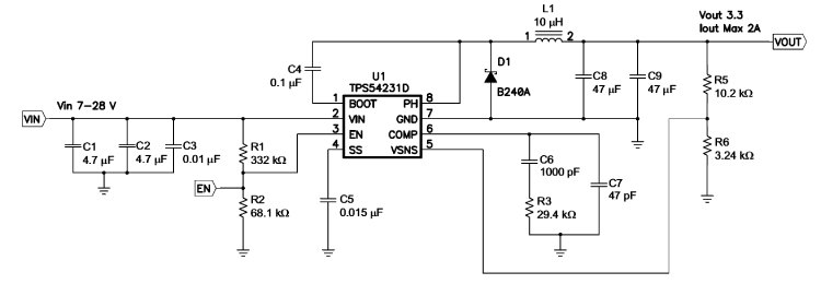
Image below shows the TPS54321D circuit diagram 3.3v output power supply using 54321 IC. You can change the output value by changing the values of feedback voltage divider resistors R5 and R6. The circuit is very simple and self-explanatory. It has the input and output filter capacitors along with the output rectifier and switching inductor. The circuit can take wide input voltage from 7V to 28V. it is capable of delivering up to 2A of current continuously.

Applications of TPS54231DR IC
- Consumer Applications such as Set-Top Boxes, CPE Equipment, LCD Displays, Peripherals, and Battery Chargers
- Industrial and Car Audio Power Supplies
- 5-V, 12-V and 24-V Distributed Power Systems.
2D-Model and Dimensions
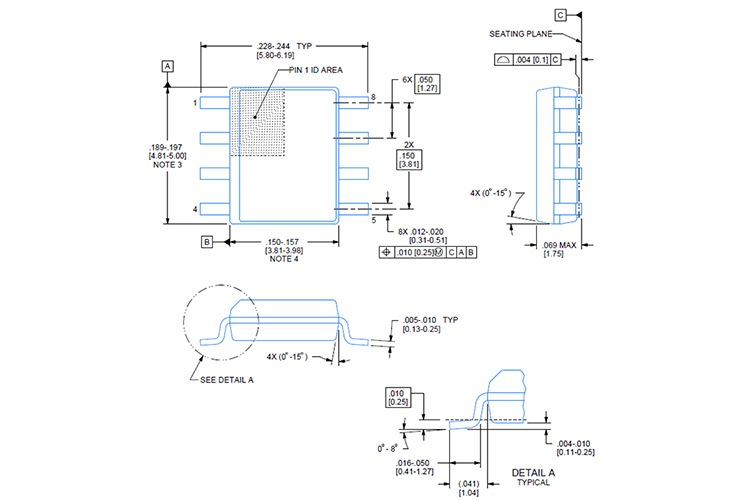
Below is the 2D CAD drawing of TPS54321D. The dimensions can be used to create custom footprints of the module and be used for PCB or CAD modelling.


