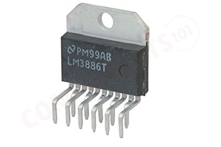
LM3886 High-Performance 68W Audio Power Amplifier
The LM3886 is a high-performance audio power amplifier which is capable of delivering 68W of continuous power with 0.1% THD+N (Total Harmonic Distortion + Noise). The peak output power of this IC is about 135 watts. The LM3886 has a unique feature called Self Peak Instantaneous Temperature (SPiKe) protection. Spike protection safeguards the amplifier against overvoltage, undervoltage, overloads, thermal runaway, and sudden temperature spikes, this makes it superior to discrete and hybrid amplifiers by ensuring a dynamically protected Safe Operating Area (SOA). This IC comes with a mute pin, we can use this pin to mute the amplifier. It has a high signal-to-noise ratio (SNR) of about 92dB and a noise floor of 2.0µV (microvolts) which helps to get more clarity and fidelity audio. This IC also offers very low THD+N values of 0.03% across the entire audio spectrum and excellent linearity with a typical IMD (SMPTE) rating of 0.004%. These properties will help to achieve high-fidelity audio reproduction.
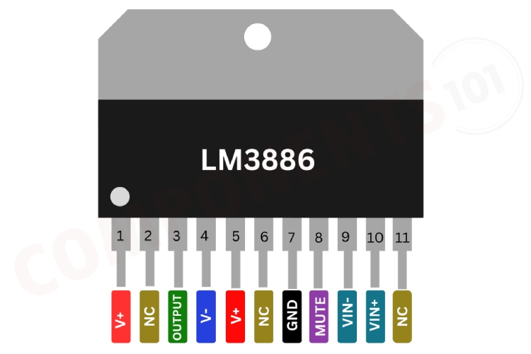
LM3886 Pinout Configuration
Here are the pinout details for LM3886.
| PIN NO | PIN NAME | DESCRIPTION |
| 1 | V+ | Positive supply voltage |
| 2 | NC | No connection |
| 3 | OUT | Audio output |
| 4 | V- | Negative supply voltage |
| 5 | V+ | Positive supply voltage |
| 6 | NC | No connection |
| 7 | GND | ground |
| 8 | MUTE | Mute pin |
| 9 | VIN- | Positive audio input |
| 10 | VIN+ | Negative audio input |
| 11 | NC | No connection |
Manufacturers of LM3886:
The LM3886 is originally manufactured by TEXAS INSTRUMENTS.
LM3886 Equivalents
There are no pin-to-pin compatible equivalents for LM3886
LM3886 Alternatives
If you are looking for an alternative for LM3886 you can look at the other ICs from these.
LM386, TDS7294, PAM8610, TDA1554, TDA2030, TDA7294, TDA7265, TDA7279, TDA2005, LA4440, TDA2002
Note: Complete technical details can be found in the LM3886 datasheet at this page’s end.
Features of LM3886
LM3886 68W power amplifier have the following key features:
- 68WCont. Avg. Output Power into 4Ω at VCC = 23 ±28V
- 38WCont. Avg. Output Power into 8Ω at VCC = ±28V
- 50WCont. Avg. Output Power into 8Ω at VCC = ±35V
- 135WInstantaneous Peak Output Power Capability
- Signal-to-Noise Ratio ≥ 92dB
- An Input Mute Function
- Output Protection from a Short to Ground or to the Supplies via Internal Current Limiting Circuitry
- Output Over-Voltage Protection against Transients from Inductive Loads
- Supply Under-Voltage Protection, not Allowing Internal Biasing to Occur when |VEE| + |VCC| ≤ 12V, thus Eliminating Turn-On and Turn-Off Transients
- 1-Lead TO-220 Package
- WideSupply Range 20V- 94V
LM3886 Schematics
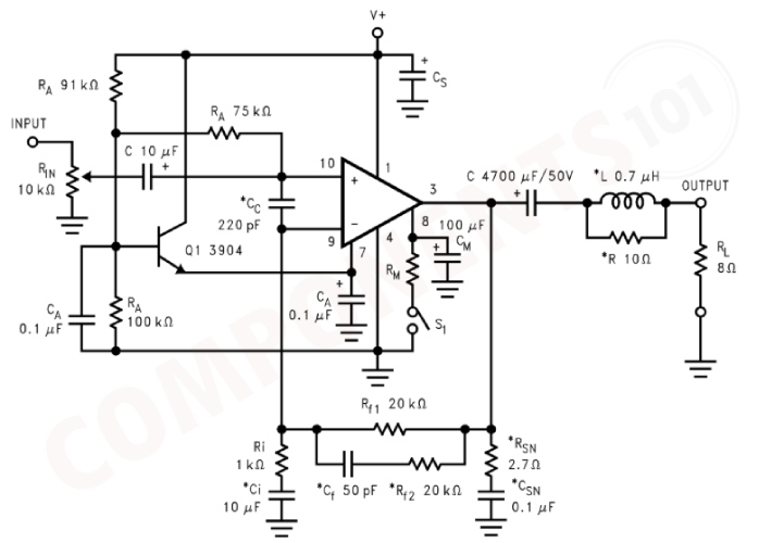
This circuit is a high-fidelity audio amplifier using the LM3886 amplifier IC. It has four major sections; the first one is the input put section. This circuit uses resistor RIN (10kΩ)to set the input impedance. The capacitor CA (0.1μF) is used to block the input DC components and allows AC signals to pass. Pins 1, 4, 7, and 8 are connected to external capacitors and resistors for stability and power supply filtering. The second section is the Feedback Network, where we used Rf1 (20kΩ) to set the gain of the amplifier. Ri (1kΩ) and Cf (50pF) are used to provide feedback network and frequency compensation. In this circuit CS (4700μF/50V) and CM (100μF) are used for power supply decoupling which provides a stable power supply to the amplifier. In the Output Stage inductor L (0.7μH) and resistor R (10Ω are connected in parallel, forming an LC network to stabilize the amplifier and prevent high-frequency oscillations.
Troubleshooting an LM3886 Circuit
My amplifier circuit is not working (not getting any sound output):
This could be due to various factors like loose connections, a muted amplifier, or a faulty source device. To find the fault first Check all cable connections between the amplifier, source device (player, phone etc.), and speakers. Ensure they're securely plugged in. Verify the values of resistors. Try it with a different source device to isolate the problem.
Getting only Distorted Sound:
Distortion can arise from blown speakers, faulty amplifier components, or clipping (an amplifier trying to output more power than it can). To solve this
- Lower the volume. Clipping often happens at high volumes.
- Check speakers for any tears or damage in the cones. Damaged speakers can cause distortion.
- If the problem persists, there might be a faulty component within the amplifier itself.
My amplifier output is very Low:
Low output could be caused by incorrect speaker impedance matching, low power input source or internal amplifier issues. To solve this
- Try changing the volume of the input source
- Verify the speaker impedance matches the amplifier's specifications. Using speakers with a much higher or lower impedance than recommended can lead to lower output.
- Check the temperature of the IC if it is high this will lead to the low output mode.
Design tips for LM3886
Is a heatsink necessary for the working of LM3886?
Yes, a heatsink is generally necessary for the proper functioning of the LM3886. The LM3886 generates heat during operation, especially when delivering higher output power. Without a heatsink, this heat can cause the IC's temperature to rise significantly.
How do we minimize the humming and buzzing sound?
A constant hum or buzz typically indicates grounding issues, faulty cables, or even interference from nearby electronics. You can follow the below steps to avoid or reduce the humming and buzzing sound.
- Ensure all the ground connections in your system are secure.
- Try using different cables to see if the culprit is a faulty cable.
- Move the amplifier away from other electronics that might be causing electrical interference.
what are the tips for designing PCB with LM3886?
- Ground Planes: Employ extensive ground planes throughout the PCB. This minimizes noise introduced by stray currents and creates a stable reference for your signal circuits.
- Trace Routing: Keep signal traces as short and direct as possible. This reduces their inductance and minimizes signal attenuation.
- Decoupling Capacitors: Place decoupling capacitors strategically near the power pins of ICs to suppress unwanted noise on the power supply lines.
- Thermal Vias: Utilize thermal vias to transfer heat from hot components to lower copper layers that can act as heat spreaders.
- Component Placement: Position heat-generating components strategically to allow for airflow and minimize thermal coupling between them.
- Trace Width and Thickness: Ensure traces have sufficient width and thickness to handle the expected current without excessive voltage drops.
- Bypass Capacitors: Utilize bypass capacitors with appropriate capacitance values placed close to the power pins of ICs to filter out high-frequency noise on the power supply.
SUPPLY BYPASSING The LM3886 has excellent power supply rejection and does not require a regulated supply. However, to eliminate possible oscillations all op amps and power op amps should have their supply leads bypassed with low inductance capacitors having short leads and located close to the package terminals. Inadequate power supply bypassing will manifest itself by a low-frequency oscillation known as “motorboating” or by high-frequency instabilities. These instabilities can be eliminated through multiple bypassing utilizing a large tantalum or electrolytic capacitor (10 μF or larger) which is used to absorb low-frequency variations and a small ceramic capacitor (0.1 μF) to prevent any high-frequency feedback through the power supply lines. If adequate bypassing is not provided the current in the supply leads which is a rectified component of the load current may be fed back into internal circuitry. This signal causes low distortion at high frequencies requiring that the supplies be bypassed at the package terminals with an electrolytic capacitor of 470 μF or more.
LEAD INDUCTANCE Power op amps are sensitive to inductance in the output lead, particularly with heavy capacitive loading. Feedback to the input should be taken directly from the output terminal, minimising common inductance with the load. Lead inductance can also cause voltage surges in the supplies. With long leads to the power supply, energy is stored in the lead inductance when the output is shorted. This energy can be dumped back into the supply bypass capacitors when the short is removed. The magnitude of this transient is reduced by increasing the size of the bypass capacitor near the IC. With at least a 20 μF local bypass, these voltage surges are important only if the lead length exceeds a couple of feet (>1 μH lead inductance). Twisting together the supply and ground leads minimizes the effect
Applications of LM3886
- Component stereo
- Compact stereo
- Self-powered speakers
- Surround-sound amplifiers
- High-end stereo TVs
- Portable Audio Systems
- Battery-Powered amplifiers
- Home Audio Systems
- Home Theaters
- Public Address Systems
- DIY Audio Projects
- Computer Audio Systems
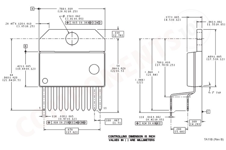
2D model and Dimensions of LM3886
Here you can find the mechanical drawings of LM3886 along with its dimensions. The dimensions can be used to create custom footprints of the module and be used for PCB or CAD modelling.