TDA1554 Audio Amplifier

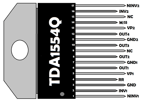
TDA1554 Pinout Configuration
|
Pin No. |
Pin Name |
Description |
|
1. |
NINV1 |
Non-inverting input 1 |
|
2. |
INV1 |
Inverting input 1 |
|
3. |
GND |
Ground (signal) |
|
4. |
RR |
Supply voltage ripple rejection |
|
5. |
VP1 |
Positive Input voltage 1 |
|
6. |
OUT1 |
Output 1 |
|
7. |
GND1 |
Power Ground 1 |
|
8. |
OUT2 |
Output 2 |
|
9. |
NC |
Not connected |
|
10. |
OUT3 |
Output 3 |
|
11. |
GND2 |
Power Ground 2 |
|
12. |
OUT4 |
Output 4 |
|
13. |
VP2 |
Positive Input voltage 2 |
|
14. |
M/SS |
Mute/Stand-by switch |
|
15. |
NC |
Not connected |
|
16. |
INV2 |
Inverting input 2 |
|
17. |
NINV2 |
Non-inverting input 2 |
Features
- Flexibility in use − Quad single-ended or stereo BTL
- High output power
- Low offset voltage at outputs (important for BTL)
- Fixed gain and Good ripple rejection
- Mute/stand-by switch
- Protected with Load Dump, Electrostatic Discharge, and Reverse Polarity
- AC and DC short-circuit-safe to ground and VP
- Thermally protected
- Capability to handle high energy on outputs (VP = 0 V)
- Low thermal resistance
- Identical inputs (inverting and non-inverting)
- Requires very few external components
Technical Specification
- Supply Voltage Range: 6V to 18V
- Output Current: 4A
- Stand-by Current: 10uA
- Total Quiescent Current: 160mA
- DC output offset voltage: 100mV
- Input Impedance: 50kΩ to75kΩ
- Supply Voltage Rejection Ratio: 48dB
Note: More technical details can be found in the TDA1554 Datasheet linked at the bottom of this page.
Brief Description
TDA1554 is a 4*11W single ended or 2*22W power amplifier IC, with an integrated Class-B output amplifier. TDA1554Q comes in a 17 lead single-in-line package. The internal circuitry contains a 4*11W single ended or 2*22W bridge amplifier. Among all four amplifiers two are inverting and other two are non-inverting. Also, each amplifier has a gain of 20dB (26dB in BTL). TDA1554q also have mute/stand-by feature.
TDA1554Q is mainly designed for car radio applications.
How to Use?
TDA1554 is an amplifier IC and can be used for designing 2*22 watt and 4*11 watt stereo audio power amplifier circuit. The circuit dissipated nearly 28 watt of heat so a good heatsink is necessary. The circuit operates at 12v and 5 amps at full volume. Reducing the volume lowers the current consumption and less heat will be dissipated.
Now, as we know we can use this IC for 2*22 watt and 4*11 watt stereo audio power amplifier circuit. The connection diagram for both are given below:
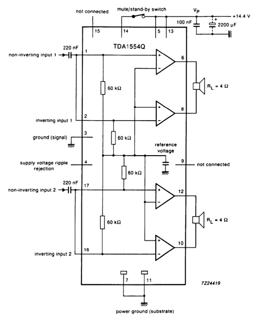
2*22 Watt Stereo Audio Power Amplifier Circuit
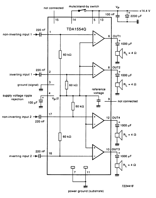
4*11 Watt Stereo Audio Power Amplifier Circuit
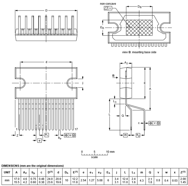
2D-Model and Dimensions