ADP2291 Compact 1.5 A Linear Charger for Single-Cell Li+ Battery
The ADP2291 is a constant-current/constant-voltage linear charger for a single-cell lithium-ion battery. ADP2291 requires a few components to operate. It has a wide 4.5 V to 12 V input voltage range. The IC supports output overshoot protection, automatic reverse isolation and thermal shutdown. Using An external, low cost, PNP we can set the charging current to the battery and an external resistor sets the maximum charge current. A small external capacitor programs the maximum charge time. The ADP2291 includes an LED driver to indicate the battery charging status. To Improve battery life, It uses an internally controlled, multistep charging cycle. This multistep charge cycle safely optimizes the battery charging time. It also provides a trickle charge mode for a deeply discharged cell and a fast-charging mode with a maximum current of 1.5 A. The ADP2291 is available in both a small, 8-pin MSOP package and a 3 × 3 mm LFCSP package that is ideally suited for small, portable applications.
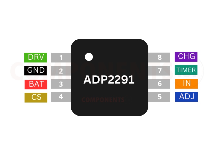
ADP2291 Pinout Configuration
Here are the pinout details for ADP2291.
| PIN | NAME | FUNCTION |
| 1 | DRV | Base Driver Output. Controls the base of an external PNP pass transistor. |
| 2 | GND | Ground. |
| 3 | BAT | Battery Voltage Sense Input |
| 4 | CS | Current Sense Resistor Negative Input. |
| 5 | ADJ | Charging Current Adjust and Charger Shutdown Input |
| 6 | IN | Power Input and Current Sense Resistor Positive Input. |
| 7 | TIMER | Timer Programming Input/Disable. |
| 8 | CHG | LED Charge Status Indicator. This is an open-collector output. |
Features of ADP2291
ADP2291 single-cell lithium-ion battery charger has the following key features:
- Simple, Safe Linear Charger for Single-Cell Lithium Battery
- 4.5 V to 12 V Input Voltage Range
- Adjustable Charging Current up to 1.5 A
- Low Cost PNP External Pass Element
- Automatic Reverse Isolation with No External Blocking Diode
- Output Overshoot Protection
- Deep Discharge Precharge Mode
- Thermal Shutdown
- Automatic Recharge
- Programmable Termination Timer
- LED Charging Status Indicator
- 4.2 V Output Voltage with ±1% Accuracy Over Line and Temperature.
- 1 µA shutdown supply current.
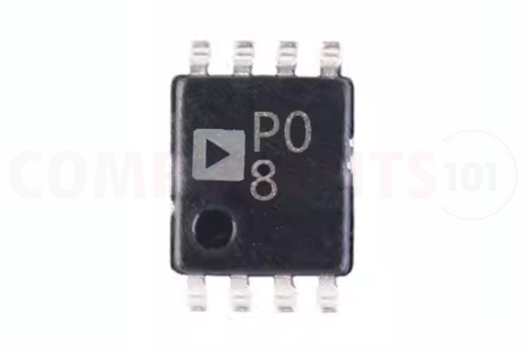
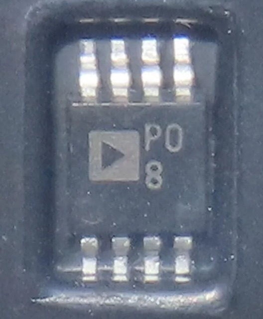
How to Identify ADP2291
The ADP2291 chips are marked with P08, regardless of the packaging. So, we can use this branding to identify the chip.
Manufacturers of ADP2291:
The ADP2291 is manufactured by Analog Devices. There are no alternative manufacturers for the same part number as of the date of writing this article.
ADP2291 Equivalents
If you are looking for an equivalent or replacement for ADP2291, we weren’t able to find any other chip that is pin-to-pin compatible.
ADP2291 Alternatives
If you are looking for an alternative for ADP2291 you can look at the other IC from these.
BQ29700, MCP7383, TP5000, TP5100 module, TP4056, MAX1898, LTC4054, BQ24074, MAX1555, LTC4054
Note: Complete technical details can be found in the ADP2291 datasheet at this page’s end.
ADP2291 Schematics
The following image shows the typical circuit diagram for ADP2291.
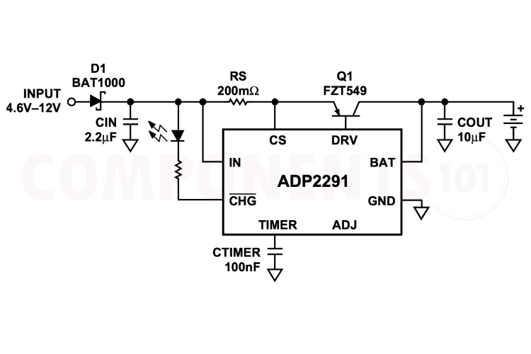
The circuit is capable of a 750-mA charge current for an input voltage of 4.5 V to 6V. Higher input voltages can be used, but the increased power dissipation of the pass device must be taken into account. As you can see the number of external components required is very few. The inputs were connected to the respective pins with a smoothing capacitor attached to them. The sense resistor connected to the CS pin determines the charging current while the capacitor connected to the TIMER pin sets the charging time. As you can see, we haven't used the ADJ pin in the circuit, and that is because we are using the internal 150mV reference for the current control. So, with this configuration, the only element that determines the current control is the current sense resistor.
Setting the Maximum Charge Current.
To set the maximum charge current, we must select a proper current sense resistor (Rs) and manage the voltage on the ADJ input. Typically, the charger maintains its output current by regulating it at a point where the voltage across the current sense resistor (V_IN – V_CS, known as V_RS) amounts to 150 mV. This reference voltage can be altered by pulling down the ADJ input, which internally connects to a 100 kΩ pull-up resistor to internal 3V. Each volt decrease from 3 V reduces VRS by 67 mV during rapid charging. When a 100 kΩ resistor links ADJ to the ground, a minimum V_RS of 50 mV is attained. During slow charge, the voltage across the current sense resistor is 15 mV with no connection to ADJ, and it drops to 10 mV with a 100 kΩ resistor attached to the ground. Therefore, the maximum charge rate IMAX is calculated as:
I_max= (V_RS (mV))/(R_s (mΩ))
Where 50 mV ≤ V_RS ≥ 150 mV.
After determining suitable values for V_RS and R_S, the value of V_ADJ and R_ADJ are calculated as
V_ADJ = (V_RS (mV) + 50 mV)/(66.7 mV) V
R_ADJ = 100 kΩ ×(V_ADJ/(3 V - V_ADJ ))
Here are some example resistor combinations for certain maximum charge currents.
| I_max | RS mΩ | VRS mV | VADJV | RADJ |
| 1.5 A | 100 | 150 | 3 | Open |
| 1 A | 100 | 100 | 2.25 | 300 K |
| 750 mA | 100 | 75 | 1.87 | 167 K |
| 500 mA | 100 | 50 | 1.5 | 100 K |
| 750 mA | 200 | 150 | 3 | Open |
| 500 mA | 200 | 100 | 2.25 | 300 K |
| 375 mA | 200 | 75 | 1.87 | 167 K |
| 250 mA | 200 | 50 | 1.5 | 100 K |
| 500 mA | 300 | 150 | 3 | Open |
| 333 mA | 300 | 100 | 2.25 | 300 K |
| 250 mA | 300 | 75 | 1.87 | 167 K |
| 167 mA | 300 | 50 | 1.5 | 100 K |
Having Troubles with ADP2291?
- The battery is not charging: Check the connections properly, and check whether the grounds of the input supply and battery are properly connected to the ground pin of the IC. Also, make sure that the battery is not flat-out dead.
- The charging current is too low: The charging current of ADP2291 is determined by the external resistor that is connected to the CS pin, check the resistor value and ensure the value is in the specified range. Also, Check the temperature of the IC, that is if the generated heat does not dissipate the charging current will be limited by the IC.
- The circuit’s performance is not stable: Use an input supply capacitor (CIN) with a value in the 1 µF to 10 µF range and place it close to the ADP2291. This should provide adequate input bypassing, but the selected capacitor should be checked in the actual application circuit. Check that the input voltage does not drop or overshoot excessively during the start-up transient. Use a battery output capacitor (COUT) with a value of at least 10 µF. This capacitance provides compensation when no battery load is present. In addition, the battery and interconnections appear inductive at high frequencies and must be accounted for when the charger is operated with a battery load. Therefore, a small amount of output capacitance is necessary to compensate for the inductive nature of the battery and connections. Use a minimum output capacitance value of 1 µF for applications where the battery cannot be removed.
Design Choices to be Considered with ADP2291:
How to add reverse polarity protection to the circuit?
To add reverse polarity protection to a circuit using the ADP2291, you can use a diode in series with the input supply. When the input supply is connected with the correct polarity, the diode conducts and allows the voltage to pass through to the ADP2291. If the input supply is connected with reverse polarity, the diode blocks the current, protecting the ADP2291 from damage.
Is a heat sink necessary for the working of ADP2291?
No. For most applications, the ADP2291 can operate without a heat sink within its specified operating conditions.
Is it possible to charge more than one battery with ADP2291?
No, the MAX18903 is designed to charge single-cell lithium-ion/polymer batteries.
What are the design considerations when designing a PCB using ADP2291?
- Keep the output capacitor as close to the BAT and GND pins as possible. Keep the input capacitor as close to the IN and GND pins as possible.
- PC board traces with larger cross-sectional areas remove more heat from the pass transistor. For optimum heat transfer, specify thick copper and use wide traces.
- Use additional copper layers or planes to reduce thermal resistance. When connecting to other layers, use multiple vias if possible.
Applications of ADP2291
- Wireless handsets
- Smart handhelds and PDAs
- Digital cameras
- Single-cell, lithium ion-powered systems
- Cradle chargers.
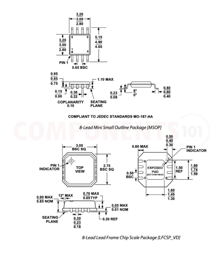
2D Model and Dimensions of ADP2291
Here you can find the mechanical drawings of ADP2291 along with its dimensions. The dimensions can be used to create custom footprints of the module and be used for PCB or CAD modelling.