ADM7171 1A Ultralow Noise CMOS LDO
The ADM7171 is an ultra-low noise, low dropout linear regulator (LDO). This IC has a high-power supply rejection ratio which helps to reduce noise in high frequency circuits. it can provide 1A continuous current and it operates from 2.3 V to 6.5 V. The IC provides thermal shutdown and current limit protection. The ADM7171 is available in 17 fixed-output voltage options ranging from 1.3V to 5V. It is available in the following standard fixed output voltages: 1.3 V, 1.8 V, 2.5 V, 3.0 V, 3.3 V, 4.2 V, and 5.0 V. The ADM7171 is also available in the following output voltage configurations by special order: 1.5 V, 1.85 V, 2.0 V, 2.2 V, 2.7 V, 2.75 V, 2.8 V, 2.85 V, 3.8 V, and 4.6 V. An adjustable version is also available that allows output voltages that range from 1.2 V to VIN − VDO with an external feedback divider. Inrush current can be controlled by adjusting the start-up time via the soft start pin. The typical start-up time with a 1 nF soft-start capacitor is 1.0 ms. The ADM7171 is available in 8-lead, 3 mm × 3 mm LFCSP package.
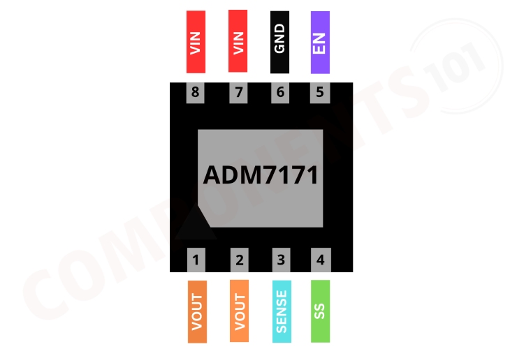
ADM7171 Pinout Configuration
Here are the pinout details for ADM7171.
| PIN | NAME | FUNCTION |
| 1 | VOUT | Regulated Output Voltage |
| 2 | VOUT | Regulated Output Voltage |
| 3 | SENSE | Sense Input |
| 4 | SS | Soft Start |
| 5 | EN | Regulator Enable |
| 6 | GND | Ground. |
| 7 | VIN | Regulator Input Supply. |
| 8 | VIN | Regulator Input Supply. |
Features of ADM7171
The ADM7171 Switching regulator has the following key features:
- Wide input voltage range: – TPS5430: 5.5V to 36V
- Up to 3A continuous (4A peak) output current
- High efficiency up to 95% enabled by 100mΩ integrated MOSFET switch
- Wide output voltage range: adjustable down to 1.22V with 1.5% initial accuracy
- Internal compensation minimises external parts count
- Fixed 500kHz switching frequency for small filter size
- Improved line regulation and transient response by input voltage feedforward
- System protected by overcurrent limiting, overvoltage protection, and thermal shutdown
- –40°C to 125°C operating junction temperature range
- Available in small thermally enhanced 8-pin SO PowerPAD™ integrated circuit package
Manufacturers of ADM7171:
ANALOG DEVICES manufactures the ADM7171. There are no alternative manufacturers for the same part number as of the date of writing this article.
ADM7171 Equivalents
There are no pin-to-pin compatible equivalents for ADM7171 you may be interested in ADM7170 with a maximum current rating of 500mA or ADM7172 with a maximum current rating of 2A.
ADM7171 Alternatives
If you are looking for an alternative for ADM7171 you can look at the other IC from these.
LM2596, XL6009, MC34063, MP9486, MP1584, TPS54231, LM2576, CS1411, LT1070, RT8059, NCP3170, LT1370, LT1765
Note: Complete technical details can be found in the ADM7171 datasheet at this page’s end.
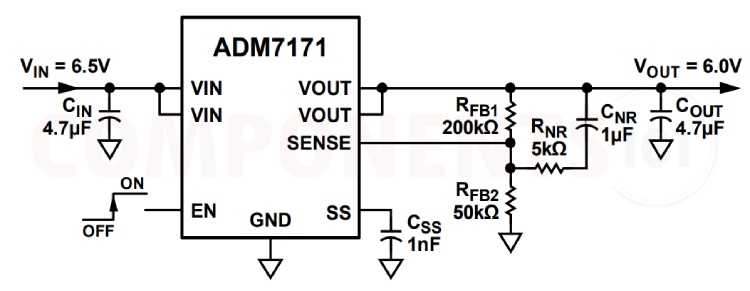
ADM7171 Circuit Diagram
The following image shows a simple circuit diagram for ADM7171.
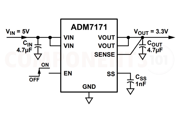
The input voltage is supplied to the VIN pins of the ADM7171. An input capacitor with a value of 4.7µF is connected between the VIN pins and ground. This capacitor helps to stabilise the input voltage and filter out any noise. The EN pin is used to enable or disable the regulator. When it is in the LOW state or connected to the ground the regulator will be shut down and the output will be disabled, when the EN pin is in the high state the LDO will be enabled and the output will be present. If the shutdown feature is not needed, then connect the En pin to the VIN pin for automatic startup. The output voltage (3.3V) is taken from the VOUT pins of the ADM7171. A 4.7µF capacitor is connected between the VOUT pin and the ground. This capacitor helps to stabilise the output voltage and filter out any noise. A 1nF capacitor is connected between the SS (Soft Start) pin and ground. This capacitor controls the startup time of the regulator, allowing for a gradual increase in the output voltage to avoid inrush current. The SENSE pin is connected to the VOUT pins. This connection allows the regulator to sense the output voltage and maintain regulation. The GND pin is connected to the ground of the circuit.
Troubleshooting Tips for ADM7171 Circuit
There is no output from the circuit. What could be the issue?
Ensure that the input supply is present and the EN pin is in the high state.
The input voltage is present and the enable pin is active. However the regulator still only gives approximately 0.6-0.8V in the output. What would be the reason?
Check if the SS pin is shorted to ground, if so, the regulator may behave like that.
ADM7171 IC is getting very hot even without load?
Check the output pin of ADM7171 first. Check whether there is any chance of a short circuit and make sure the pad is connected to the ground. If the problem persists, try to change the ADM7171.
I'm experiencing a lot of ripples on the ADM7171 output. What might be causing this?
Make sure to use the appropriate filter capacitor at the input and output.
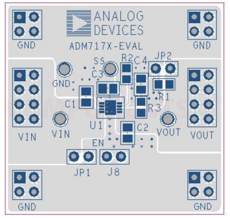
Things to Consider When Using ADM7171 in Your Design
Layout Guidelines
Heat dissipation from the package can be improved by increasing the amount of copper attached to the pins of the ADM7171. However, as listed in Table 7, a point of diminishing returns is eventually reached, beyond which an increase in the copper size does not yield significant heat dissipation benefits. Place the input capacitor as close as possible to the VIN and GND pins. Place the output capacitor as close as possible to the VOUT and GND pins. The use of 0805 or 1206 size capacitors and resistors achieves the smallest possible footprint solution on boards where the area is limited. Here is an example PCB layout.
EFFECT OF NOISE REDUCTION ON START-UP TIME
The start-up time of the ADM7171 is affected by the noise reduction network and must be considered in applications wherein power supply sequencing is critical. The noise reduction circuit adds a pole in the feedback loop that slows down the start-up time. The start-up time for an adjustable model with a noise reduction network can be approximated using the following equation:
SSNRTIME (sec) = 5.5 × CNR × (RNR + RFB1)
For a CNR, RNR, and RFB1 combination of 1 μF, 5 kΩ, and 200 kΩ, respectively, as shown in the below figure, the start-up time is approximately 1.1 seconds. When SSNRTIME is greater than SSTIME, it dictates the length of the start-up time instead of the soft start capacitor.
Applications of ADM7171
- Set-top box
- DVD Players
- LCD displays
- Industrial and car audio power supplies
- Battery chargers
- High-power LED supply
- 12V and 24V distributed power systems
Ordering Information for ADM7171
The ADM7171 can be ordered with the following parts numbers ADM7171ACPZ-R7 and ADM7171ACPZ-R2 are adjustable variants, and all other fixed voltage variants will have the part number in the following format: ADM7171ACPZ-x.x-R7, where the x.x denotes the output voltage. For example, ADM7171ACPZ-3.3-R7 represents the 3.3V regulator while ADM7171ACPZ-5.0-R7 represents the 5V regulator.
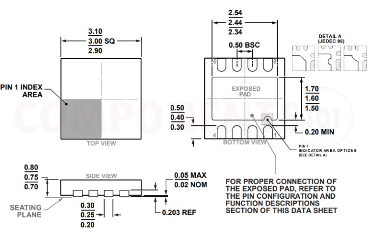
2D Model and Dimensions of ADM7171
Here you can find the mechanical drawings of ADM7171 along with its dimensions. The dimensions can be used to create custom footprints of the IC and be used for PCB or CAD modelling.