MIC5205 Low Noise 150mA LDO
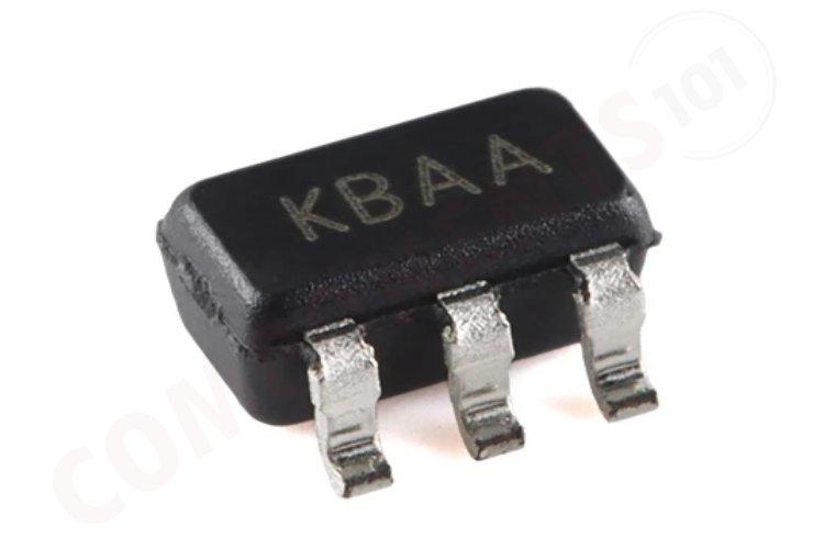
The MIC5205 is an ultra-small, highly efficient linear voltage regulator available in both adjustable and fixed output voltage variants. This small IC offers ultra-low-noise output, very low dropout voltage and very low ground current. The IC has a CMOS or TTL-compatible enable/shutdown control input. This IC requires only filtering capacitors to work properly. When shut down, power consumption drops nearly to zero. Due to its low noise performance and low dropout voltage, MIC5205 is perfect for battery-operated analog devices. MIC5205 provides a reference bypass pin to improve its already excellent low-noise performance, reversed-battery protection, current limiting, and overtemperature shutdown. The MIC5205 is available in a small SOT-23-5 package.
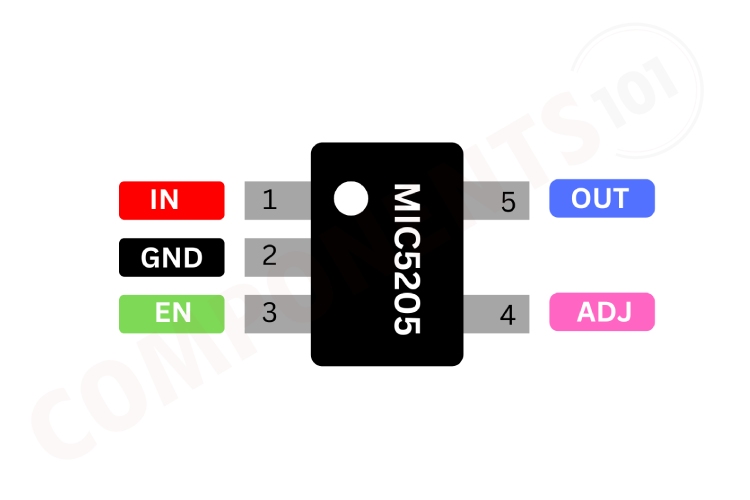
MIC5205 Pinout Configuration
Here are the pinout details for MIC5205.
| PIN NO | NAME | FUNCTION |
| 1 | IN | Input voltage |
| 2 | GND | Ground |
| 3 | EN | Enable pin |
| 4 | ADJ | Voltage Adjustment |
| 5 | OUT | Output voltage |
Features of MIC5205
The MIC5205 Switching regulator has the following key features:
- Ultra-Low Noise Output
- High Output Voltage Accuracy Guaranteed 150 mA Output
- Low Quiescent Current
- Low Dropout Voltage
- Extremely Tight Load and Line Regulation
- Very Low-Temperature Coefficient
- Current and Thermal Limiting
- Reverse-Battery Protection
- Zero Off-Mode Current
- Logic-Controlled Electronic Enable
Manufacturers of MIC5205:
MIC5205 is manufactured by Microchip Technologies. There are no alternative manufacturers for the same part number as of the date of writing this article.
MIC5205 Equivalents
If you are looking for a pin-to-pin compatible equivalent for MIC5205, consider using any of the following parts SPX5205, SGM2019 or RT9080.
MIC5205 Alternatives
If you are looking for an alternative for MIC5205 you can look at the other ICs from these.
LM2596, XL6009, MC34063, MP9486, MP1584, TPS54231, LM2576, CS1411, LT1070, RT8059, NCP3170, LT1370, LT1765, TPS5430
Note: Complete technical details can be found in the MIC5205 datasheet at this page’s end.
MIC5205 Circuit Diagram
The following image shows a simple circuit diagram for MIC5205.
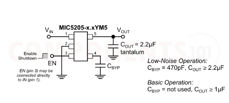
This above circuit is a typical application circuit of MIC5205. The circuit provides stable voltage out from a 2.5-16v input.
In this circuit, unregulated input is supplied to the VIN pin. Pin to is connected to common ground. Enable pin can be used to turn the regulator on or off. If this pin is connected to VIN, the regulator is enabled (ON). If it is connected to GND, the regulator is disabled (OFF). A bypass pin is used to reduce the output noise further. The capacitor is used to improve the regulator’s noise performance. For low-noise operation, a 470 pF capacitor should be connected between CBYP and GND. For basic operation, this capacitor is not required. VOUT is the Output voltage. A capacitor with a value of at least 1 µF should be connected between VOUT and GND to ensure stability. For low-noise operation, a capacitor with a value of at least 2.2 µF (tantalum) is recommended.
Troubleshooting Tips for MIC5205 Circuit
There is no output from the circuit. What could be the issue?
First, ensure that the power supply voltage and current are sufficient. Check the connections to the MIC5205. Make sure the EN pin is high.
MIC5205 IC is getting very hot even without load?
Check the output pin of MIC5205 first. Check whether there is any chance of a short circuit. If the problem persists, try to change the MIC5205.
I'm experiencing a lot of ripples on the MIC5205 output. What might be causing this?
Make sure to use the appropriate filter capacitor at the input and output. For low-noise operation, a capacitor with a value of at least 2.2 µF (tantalum) is recommended
Things to Consider When Using MIC5205 in Your Design
Enable/Shutdown- Forcing EN (enable/shutdown) high (greater than 2V) enables the regulator. EN is compatible with CMOS logic gates. If the enable/shutdown feature is not required, connect EN (pin 3) to IN (supply input, pin 1).
Input Capacitor 1 µF capacitor should be placed from IN to GND if there are more than 10 inches of wire between the input and the AC filter capacitor or if a battery is used as the input.
Reference Bypass Capacitor- BYP (reference bypass) is connected to the internal voltage reference. A 470 pF capacitor (CBYP) connected from BYP to GND quiets this reference, providing a significant reduction in output noise. CBYP reduces the regulator phase margin; when using CBYP, output capacitors of 2.2 µF or greater are generally required to maintain stability. The start-up speed of the MIC5205 is inversely proportional to the size of the reference bypass capacitor. Applications requiring a slow ramp-up of output voltage should consider larger values of CBYP. Likewise, if a rapid turn-on is necessary, consider omitting CBYP. If output noise is not a major concern, omit CBYP and leave BYP open.
Output Capacitor- An output capacitor between OUT and GND is required to prevent oscillation. The minimum size of the output capacitor is dependent upon whether a reference bypass capacitor is used. 1.0 µF minimum is recommended when CBYP is not used. A 2.2 µF minimum is recommended when CBYP is 470 pF. Larger values improve the regulator’s transient response. The output capacitor value may be increased without limit. The output capacitor should have an ESR (effective series resistance) of about 5Ω or less and a resonant frequency above 1 MHz. Ultra-low-ESR capacitors can cause a low amplitude oscillation on the output and/or underdamped transient response. Most tantalum or aluminum electrolytic capacitors are adequate; film types will work, but are more expensive. Because many aluminium electrolytics have electrolytes that freeze at about –30°C, solid tantalums are recommended for operation below –25°C. At lower values of output current, less output capacitance is required for output stability. The capacitor can be reduced to 0.47 µF for a current below 10 mA or 0.33 µF for a current below 1 mA.
No-Load Stability- The MIC5205 will remain stable and in regulation with no load (other than the internal voltage divider) unlike many other voltage regulators. This is especially important in CMOS RAM keep-alive applications.
Thermal Considerations- The MIC5205 is designed to provide 150 mA of continuous current in a very small package. Maximum power dissipation can be calculated based on the output current and the voltage drop across the part. To determine the maximum power dissipation of the package, use the junction-to-ambient thermal resistance of the device and the following basic equation:
PD MAX = (TJ MAX) -( TA ) / θ JA
TJ(MAX) is the maximum junction temperature of the die, 125°C, and TA is the ambient operating temperature. θJA is layout dependent.
Applications of MIC5205
- Cellular Telephones
- Laptop, Notebook, and Palmtop Computers
- Battery-Powered Equipment
- PCMCIA VCC and VPP Regulation/Switching
- Consumer/Personal Electronics
- SMPS Post-Regulator and DC/DC Modules
- High-Efficiency Linear Power Supplies
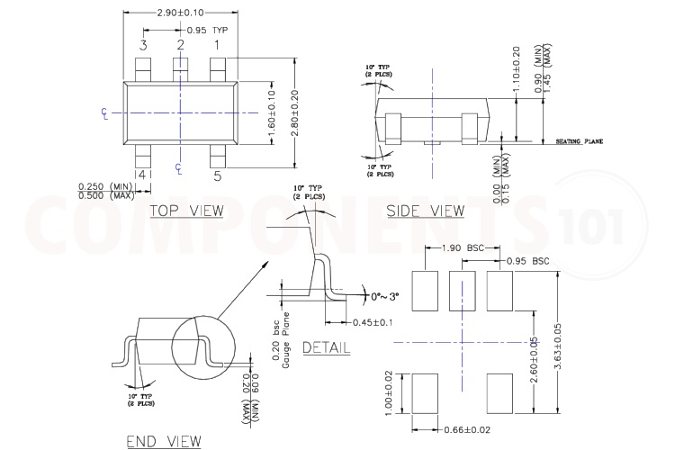
2D Model and Dimensions of MIC5205
Here you can find the mechanical drawings of MIC5205 along with its dimensions. The dimensions can be used to create custom footprints of the IC and be used for PCB or CAD modelling.