NCP3170 – Synchronous Buck Regulator
The NCP3170 is a synchronous buck regulator with integrated switching elements. It has a wide Input Voltage Range from 4.5V to 18V and it can deliver up to 3A output current. The NCP3170 uses current mode control for fast transient response and easy loop compensation. The output voltage can be adjusted from 0.8 volts to the maximum input voltage. The NCP3170 switching frequency is fixed at 500KHz (for NCP3170A, and for NCP3170B it is 1MHz) and set by an internal oscillator. This small IC comes with safety features such as soft start, short circuit protection, thermal shutdown and power good indication. Because of the integrated switching element and the built-in safety feature this regulator IC requires only bare minimum components. The IC also offers over-current protection, over-voltage protection and thermal shutdown. The NCP3170 is available in an SOIC−8 package.
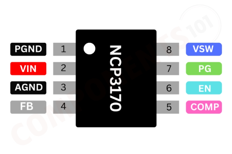
NCP3170 Pinout Configuration
Here are the pinout details for NCP3170.
| Pin | Pin Name | Description |
| 1 | PGND | power ground |
| 2 | VIN | Input supply |
| 3 | AGND | Analog ground |
| 4 | FB | The FB pin in conjunction with the external compensation serves to stabilize and achieve the desired output voltage with current mode compensation. |
| 5 | COMP | The loop compensation pin is used to compensate the transconductance amplifier which stabilizes the operation of the converter stage. |
| 6 | EN | Enable pin |
| 7 | PG | Power good is an open drain 500 µA pull down indicating output voltage is within the power good window |
| 8 | VSW | The VSW pin is the connection of the drains of the internal N and P MOSFETS. |
Features of NCP3170
The NCP3170 Switching regulator has the following key features:
- 4.5 V to 18 V Operating Input Voltage Range
- 90 m High-Side, 25 m Low-Side Switch
- FMEA Fault Tolerant During Pin Short Test
- 3 A Continuous Output Current
- Fixed 500 kHz and 1 MHz PWM Operation
- Cycle-by-Cycle Current Monitoring \
- 1.5% Initial Output Accuracy
- Internal 4.6 ms Soft-Start
- Short-Circuit Protection
- Turn on Into Pre-bias
- Power Good Indication
- Light Load Efficiency
- Thermal Shutdown
- These are Pb-Free Devices
Manufacturers of NCP3170:
The NCP3170 is manufactured by On Semiconductor. There are no alternative manufacturers for the same part number as of the date of writing this article.
NCP3170 Variants
The NCP3170 has two variants- NCP3170A with 500KHz switch frequency and NCP3170B with 1MHz switching frequency. Both are available with the part numbers NCP3170ADR2G and NCP3170BDR2G.
NCP3170 Equivalents
There are no pin-to-pin compatible equivalents for NCP3170
NCP3170 Alternatives
If you are looking for an alternative for NCP3170 you can look at the other IC from these.
LM2596, XL6009, MC34063, MP9486, MP1584, TPS54231, LM2576, CS1411, LT1070, RT8059, TPS5430, LT1765, LT1370
Note: Complete technical details can be found in the NCP3170 datasheet at this page’s end.
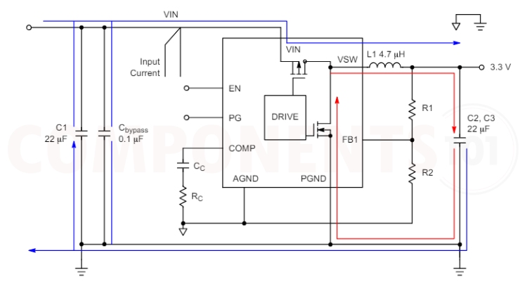
NCP3170 Circuit Diagram
The following image shows a simple circuit diagram for NCP3170.
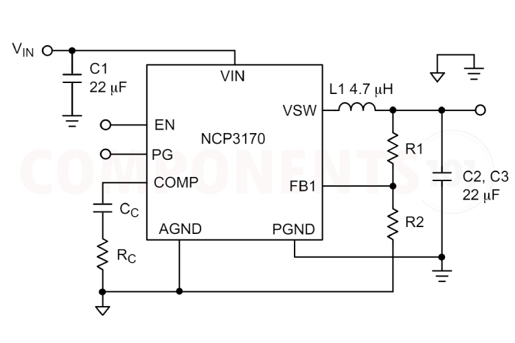
This above circuit is a typical application circuit of NCP3170. In this circuit 1 input is supplied to the VIN pin The C1 capacitor filters the input voltage (VIN), reduces noise and stabilizes the input voltage. The EN pin is used to enable or disable the converter. When connected to a high voltage, the converter is enabled; when connected to a low voltage, it is disabled. The Power Good pin is an open-drain output that indicates the status of the output voltage. It is typically connected to a pull-up resistor to an external voltage. compensation pin is used for compensation of the control loop to ensure stability. It is connected to the RC network. AGND is the ground reference for the analog circuitry of the converter.
Power Ground is the ground reference for the power stage of the converter. Both grounds should be connected together at a single point to minimize noise. The inductor stores energy when the switch is on and releases it when the switch is off, smoothing the output current and reducing ripple. C2 and C3 capacitors filters the output voltage to reduce noise and stabilize the output voltage.
R1 and R2 resistors form a voltage divider network that sets the output voltage. The voltage at the feedback pin (FB1) is compared to a reference voltage (typically 0.8V) to regulate the output.
For calculating the values of the resistors used in the voltage divider the following formula can be used.
R_2=R_1×(V_REF/(V_OUT-V_REF )) where V_REF= 0.8V
Here are some of the most common output voltages and the voltage divider combination for them.
| VO (V) | R1 (kΩ) | R2 (kΩ) |
| 0.8 | 24.9 | Open |
| 1 | 24.9 | 100 |
| 1.1 | 24.9 | 66.5 |
| 1.2 | 24.9 | 49.9 |
| 1.5 | 24.9 | 28.7 |
| 1.8 | 24.9 | 20 |
| 2.5 | 24.9 | 11.8 |
| 3.3 | 24.9 | 8.06 |
| 5 | 24.9 | 4.64 |
Troubleshooting Tips for NCP3170 Circuit
There is no output from the circuit. What could be the issue?
Make sure the EN pin is high and has a voltage level above 4.41V.
How to archive adjustable under-voltage lockout?
To enable under-voltage lockout, use a voltage divider to pull up the EN pin instead of tying it directly to the Vin. The trip voltage for the EN pin comparator is 1.38V. If large resistor values are used, the EN pin should be bypassed with a 1 nF capacitor to prevent coupling problems from the switch node.
I'm experiencing a lot of ripples on the NCP3170 output. What might be causing this?
Make sure to use the appropriate filter capacitor at the output.
Things to Consider When Using NCP3170 in your Design
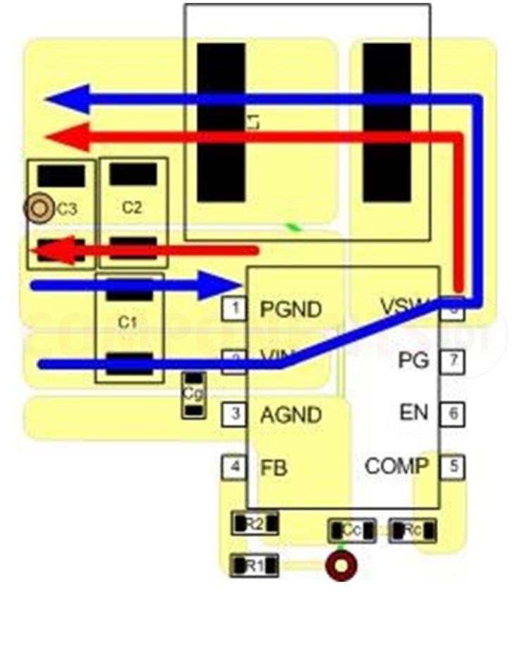
THERMAL MANAGEMENT AND LAYOUT
In the NCP3170 buck regulator high pulsing current flows through two loops as shown in the figure below.
The first loop shown in blue activates when the high side switch turns on. When the switch turns on, the edge of the current waveform is provided by the bypass capacitor. The remainder of the current is provided by the input capacitor. Slower currents are provided by the upstream power supply which fills up the input capacitor when the high side switch is off. The current flows through the high side MOSFET and to the output, charging the output capacitors and providing current to the load. The current returns through a PCB ground trace where the output capacitors are connected, the regulator is grounded, and the input capacitors are grounded. The second loop starts from the inductor to the output capacitors and load and returns through the low-side MOSFET. Current flows in the second loop when the low-side NMOSFET is on. The designer should note that there are locations where the red line and the blue line overlap; these areas are considered to have DC current. Areas containing a single blue line indicate that AC currents flow and transition very quickly. The key to the power supply layout is to focus on the connections where the AC current flows. A good rule of thumb is that for every inch of PCB trace, 20 nH of inductance exists. When laying out a PCB, minimizing the AC loop area reduces the noise of the circuit and improves efficiency. A ground plane is strongly recommended to connect the input capacitor, output capacitor, and PGND pin of the NCP3170. Drawing the real high-power current flow lines on the recommended layout is important so the designer can see where the currents are flowing.
The NCP3170 is the major source of power dissipation in the system for which the equations above detailed the loss mechanisms. The control portion of the IC power dissipation is determined by the formula below:
PC=Ic* VIN (eq. 52)
where:
ICC = Control circuitry current draw
PC = Control power dissipation
VIN = Input voltage
Once the IC power dissipations are determined, the designer can calculate the required thermal impedance to maintain a specified junction temperature at the worst-case ambient temperature. The formula for calculating the junction temperature with the package in free air is:
TJ = TA + PD × RθJA (eq. 53)
where:
PD = Power dissipation of the IC
RθJA = Thermal resistance junction to ambient of the regulator package
TA = Ambient temperature
TJ = Junction temperature
The thermal performance of the NCP3170 is strongly affected by the PCB layout. Extra care should be taken by users during the design process to ensure that the IC will operate under the recommended environmental conditions. As with any power design, proper laboratory testing should be performed to ensure the design will dissipate the required power under worst-case operating conditions. Variables considered during testing should include maximum ambient temperature, minimum airflow, maximum input voltage, maximum loading, and component variations (i.e., worst-case MOSFET RDS(on)). Several layout tips are listed below for the best electric and thermal performance. The Image below illustrates a PCB layout example of the NCP3170.
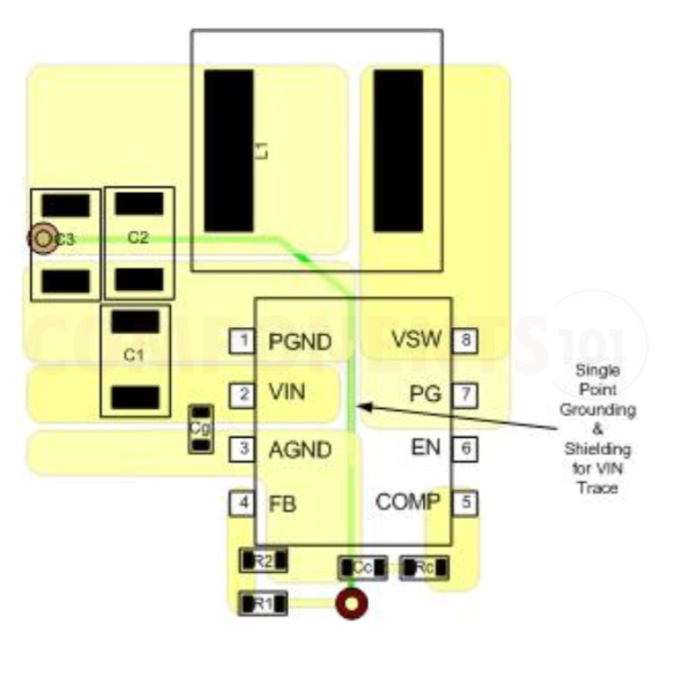
- The VSW pin is connected to the internal PFET and NFET drains, which are a low-resistance thermal path. Connect a large copper plane to the VSW pin to help thermal dissipation. If the PG pin is not used in the design, it can be connected to the VSW plane, further reducing the thermal impedance. The designer should ensure that the VSW thermal plane is rounded at the corners to reduce noise
- The user should not use thermal relief connections to the VIN and the PGND pins. Construct a large plane around the PGND and VIN pins to help thermal dissipation.
- The input capacitor should be connected to the VIN and PGND pins as close as possible to the IC.
- A ground plane on the bottom and top layers of the PBC board is preferred. If a ground plane is not used, separate PGND from AGND and connect them only at one point to avoid the PGND pin noise coupling to the AGND pin. 5. Create copper planes as short as possible from the VSW pin to the output inductor, from the output inductor to the output capacitor, and from the load to PGND. 6. Create a copper plane on all of the unused PCB area and connect it to stable DC nodes such as VIN, GND, or VOUT. 7. Keep sensitive signal traces far away from the VSW pins or shield them.
Applications of NCP3170
- Set Top Boxes
- DVD/Blu−ray Drives and HDD
- LCD Monitors and TVs
- Cable Modems
- PCIe Graphics Cards
- Telecom/Networking/Datacom Equipment
- Point of Load DC/DC Converters
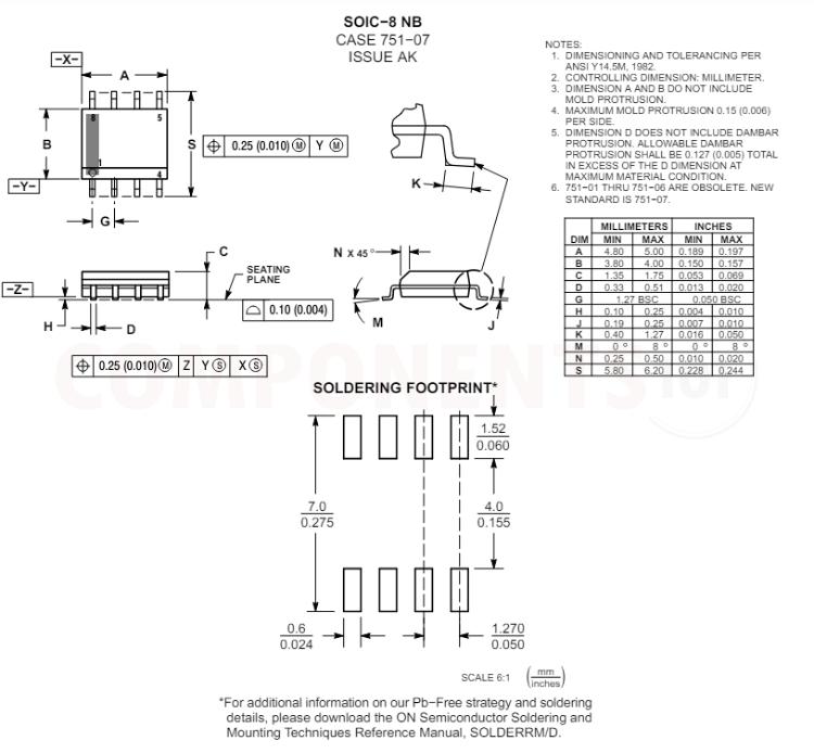
2D Model and Dimensions of NCP3170
Here you can find the mechanical drawings of NCP3170 along with its dimensions. The dimensions can be used to create custom footprints of the IC and be used for PCB or CAD modelling.