MCP4728 12-Bit, Quad Digital-to-Analog Converter
The MCP4728 is a quad, 12-bit, I2C enabled, voltage output Digital-to-Analog Converter (DAC) with EEPROM. It has rail-to-rail output swing capability, which is quite useful, especially in applications where you need to drive signals close to the power supply rails. With the help of Its onboard precision output amplifier, MCP4728 can achieve rail-to-rail analog output swing. We can program the DAC input codes, device configuration bits, and I2C address bits to nonvolatile memory using the I2C serial interface commands simplifies the setup and configuration process. The device has a high-precision internal voltage reference. We can set the channels into normal mode and power down mode separately also we can select the internal reference or external reference for each channel individually. The MCP4728 has a two-wire I2C compatible serial interface for standard (100 kHz), fast (400 kHz), or high-speed (3.4 MHz) modes. The MCP4728 device is available in a 10-lead MSOP package and operates from a single 2.7V to 5.5V supply voltage.
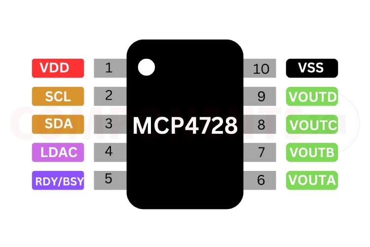
MCP4728 Pinout Configuration
Here are the pinout details for MCP4728.
| Pin No | Name | Function |
| 1 | VDD | Supply Voltage |
| 2 | SCL | I2C Serial Clock Input |
| 3 | SDA | I2C Serial Data Input and Output |
| 4 | LDAC | This pin is used for two purposes: (a) Synchronization Input. It is used to transfer the contents of the DAC input registers to the output registers (VOUT). (b) Select the device for reading and writing I2C address bits. |
| 5 | RDY/BSY | This pin is a status indicator of EEPROM programming activity. |
| 6 | VOUT A | Buffered analog voltage output of channel A. |
| 7 | VOUT B | Buffered analog voltage output of channel B. |
| 8 | VOUT C | Buffered analog voltage output of channel C. |
| 9 | VOUT D | Buffered analog voltage output of channel D. |
| 10 | VSS | Ground reference. |
Features of MCP4728
MCP4728 ADC chip has the following key features:
- 12-bit Voltage Output DAC with Four Buffered Outputs
- On-board nonvolatile Memory (EEPROM) for DAC Codes and I2C Address Bits
- Internal or External Voltage Reference Selection
- Output Voltage Range: - Using Internal VREF (2.048V): 0.000V to 2.048V with Gain Setting = 1 0.000V to 4.096V with Gain Setting = 2 - Using External VREF (VDD): 0.000V to VDD
- ±0.2 Least Significant Bit (LSB) Differential Nonlinearity (DNL) (typical)
- Fast Settling Time: 6 µs (typical)
- Normal or Power-Down Mode
- Low Power Consumption
- Single-Supply Operation: 2.7V to 5.5V
- I2C Interface: - Address bits: User Programmable to EEPROM - Standard (100 kbps), Fast (400 kbps) and High Speed (HS) Mode (3.4 Mbps)
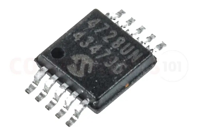
- 10-Lead MSOP Package
- Extended Temperature Range: -40°C to +125°C
Manufacturers of MCP4728:
The MCP4728 is manufactured by microchip technologies. There are no alternative manufacturers for the same part number as of the date of writing this article.
MCP4728 Equivalents
There is no equivalent replacement for MCP4728.
MCP4728 Alternatives
If you are looking for an alternative for MCP4728 you can look at the other IC from these.
DAC8562, MCP4725, MCP4921, PT8211, DAC0832, DAC0808, DAC7715, AD5737, MAX5216, MCP4922
Note: Complete technical details can be found in the MCP4728 datasheet at this page’s end.
MCP4728 Typical Circuit Diagram
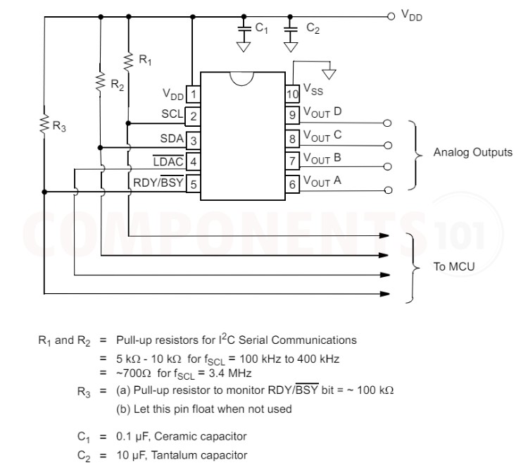
The above circuit shows how to connect an MCP4728 with a microcontroller.
The SCL, SDA, and RDY/BSY pins of the MCP4728 device are open-drain configurations. These pins require a pull-up resistor. The LDAC pin has a Schmitt trigger input configuration and it can be driven by an external MCU I/O pin. The pull-up resistor values (R1 and R2) for SCL and SDA pins depend on the operating speed (standard, fast, and high speed) and loading capacitance of the I 2C bus line. A higher value of pull-up resistor consumes less power but increases the signal transition time (higher RC time constant) on the bus line. Therefore, it can limit the bus operating speed. A lower resistor value, on the other hand, consumes higher power but allows for higher operating speed. If the bus line has higher capacitance due to long metal traces or multiple device connections to the bus line, a smaller pull-up resistor is needed to compensate for the long RC time constant. The pull-up resistor is typically chosen between 1 kΩ and 10 kΩ range for standard and fast modes, and less than 1 kΩ for high-speed mode.
MCP4728 Troubleshooting Guide
My MCP4728 is not providing any output. What could be the issue?
First, ensure that the power supply voltages are within the specified range (2.7V to 5.5V). Check the connections to the MCP4728, including VSS, VDD, and the I2C pins.
How to check my circuit connections are correct?
You can use the I2C scanner code to check whether the device is detected or not.
How to do MCP4728 Arduino interfacing?
The MCP4728 uses an I2C protocol for communication. So, you can use the I2C pins of Arduino to communicate with the MCP4728. You can use the MCP4728 library for easy interfacing. More details about the I2C communication can be found in the datasheet.
Are there any evaluation boars available for MCP4728?
The MCP4728 Evaluation Board is available from Microchip Technology Inc. This board works with Microchip’s PICkit Serial Analyzer. The user can easily program the DAC input registers and EEPROM using the PICkit Serial Analyzer and test out the DAC analog output voltages. The PICkit Serial Analyzer uses the PC Graphic User Interface software. Refer to www.microchip.com for further information on this product’s capabilities and availability.
Things to Consider When Using MCP4728 in Your Design.
When designing with the MCP4728, a 12-bit Analog-to-Digital Converter (ADC), here are some important considerations and design tips to keep in mind:
Layout Considerations
Inductively coupled AC transients and digital switching noise from other devices can affect DAC performance and DAC output signal integrity. A careful board layout will minimize these effects. Bench testing has shown that a multi-layer board utilizing a low-inductance ground plane, isolated inputs, isolated outputs and proper decoupling are critical to achieving good DAC performance. Separate digital and analog ground planes are recommended. In this case, the VSS pin and the ground pins of the VDD capacitors of the MCP4728 should be terminated to the analog ground plane.
Power Supply Considerations
The power source should be as clean as possible. The power supply to the device is used for both VDD and DAC voltage reference by selecting VREF = VDD. Any noise induced on the VDD line can affect DAC performance. A typical application will require a bypass capacitor in order to filter out high-frequency noise on the VDD line. The noise can be induced onto the power supply’s traces or as a result of changes in the DAC output. The bypass capacitor helps to minimize the effect of these noise sources on signal integrity. Should connect two bypass capacitors (a 10 µF tantalum capacitor and a 0.1 µF ceramic capacitor) in parallel on the VDD line. These capacitors should be placed as close to the VDD pin as possible (within 4 mm). If the application circuit has separate digital and analog power supplies, the VDD and VSS pins of the MCP4728 device should reside on the analog plane.
Applications of MCP4728
- Set Point or Offset Adjustment
- Sensor Calibration
- Closed-Loop Servo Control
- Low Power Portable Instrumentation
- PC Peripherals
- Programmable Voltage and Current Source
- Industrial Process Control
- Instrumentation
- Bias Voltage Adjustment for Power Amplifiers
MCP4728 Ordering Information
The MCP4728 can be ordered using the following part numbers, MCP4728-E/UN, MCP4728T-E/UN, MCP4728A0-E/UN, MCP4728A0T-E/UN, MCP4728A1-E/UN, MCP4728A1T-E/UN, MCP4728A2-E/UN, MCP4728A2T-E/UN, MCP4728A3-E/UN, MCP4728A3T-E/UN, MCP4728A4-E/UN, MCP4728A4T-E/UN, MCP4728A5-E/UN, MCP4728A5T-E/UN, MCP4728A6-E/UN, MCP4728A6T-E/UN, MCP4728A7-E/UN, MCP4728A7T-E/UN. All of them are the same and have the same footprint. The device marking may be different for each.
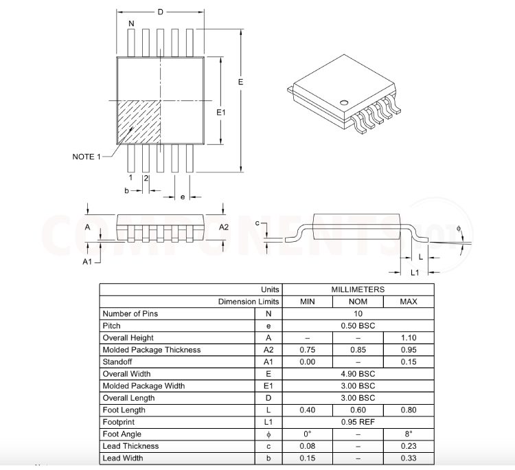
MCP4728 Footprint Information
Here you can find the mechanical drawings of MCP4728 along with its dimensions. The dimensions can be used to create custom footprints of the module and be used for PCB or CAD modelling.