DAC8562 Dual 12-Bit, Low-Power, Buffered, Voltage-Output DAC


The DAC8562 is a low-cost 12-bit, parallel input, voltage output Digital to Analog converter (DAC). This DAC is based on the complementary Bipolar-CMOS (CBCMOS) process. This DAC is designed to operate in systems that use only a +5-volt power supply. The DAC8562 also includes a rail-to-rail amplifier, a latch, and a reference voltage source (REFOUT). The reference voltage is trimmed to 2.5 volts, and an on-chip amplifier scales the DAC output to 4.095 volts full scale. This integration simplifies the design for users, as they only need to supply a positive voltage. The DAC8562 is coded straight binary. DAC8562 offers monotonic performance, ensuring excellent linearity and minimizing unwanted code-to-code transient voltages (glitches). It uses a versatile three-wire serial interface that can operate at clock rates up to 50 MHz, providing fast and efficient communication with the device. The interface is compatible with standard SPI, QSPI, microwire, and digital signal processor interfaces. It has a power-down feature that reduces current consumption to typically 550 nA at 5 V. The low power consumption, internal reference and small footprint make these devices ideal for portable, battery-operated equipment. The DAC8562 is available in MSOP-10 and SON-10 packages.
DAC8562 Pinout Configuration:
Here are the pinout details for DAC8562.
| Pin Number | Name | Function |
| 1 | V OUTA | Analog output voltage from DAC-A |
| 2 | V OUT B | Analog output voltage from DAC-B |
| 3 | GND | Ground |
| 4 | LDAC | LDAC |
| 5 | CLR | Asynchronous Clear input |
| 6 | SYNC | Level-triggered control input |
| 7 | SCLK | Serial Clock input |
| 8 | DIN | Serial data input |
| 9 | AVDD | 2.7V to 5.5V Power Supply |
| 10 | VREF | Bidirectional voltage reference pin |
Features of DAC8562:
DAC8562 ADC chip has the following key features:
- Glitch Impulse: 0.1 nV-s
- Bidirectional Reference: Input or 2.5-V Output
Output Disabled by Default
±5-mV Initial Accuracy (Max)
4-ppm°C Temperature Drift (Typ)
10-ppm/°C Temperature Drift (Max)
20-mA Sink and Source Capability
- Power-On Reset to Zero Scale or Mid-Scale
- Low-Power: 4 mW (Typ, 5-V AVDD, Including Internal Reference Current)
- Wide Power-Supply Range: 2.7 V to 5.5 V
- 50-MHz SPI With Schmitt-Triggered Inputs
- LDAC and CLR Functions
- Output Buffer with Rail-to-Rail Operation
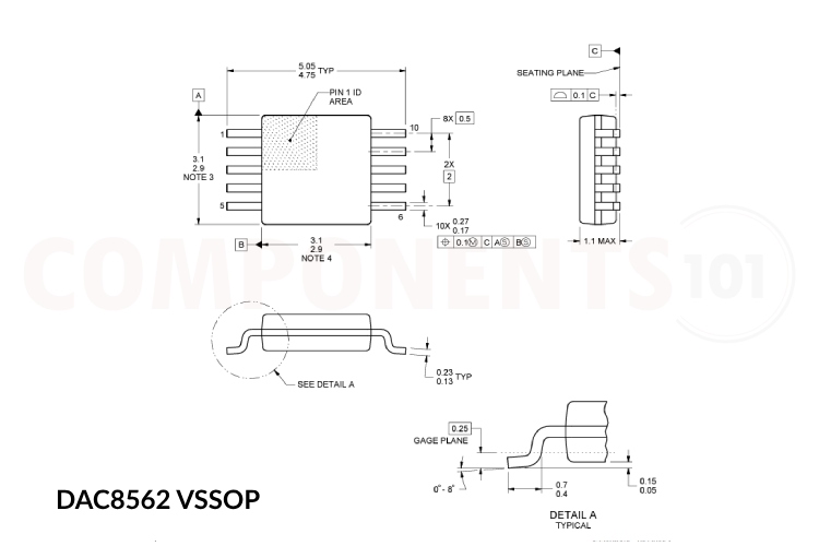
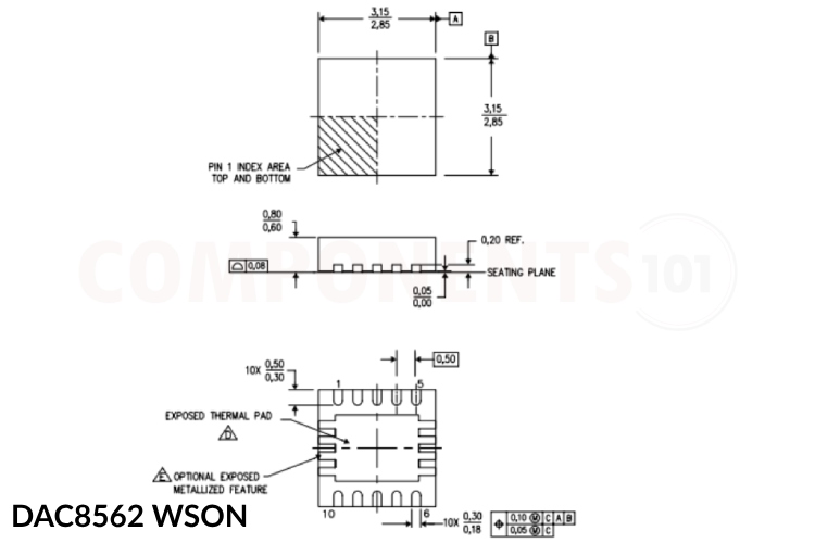
- Packages: WSON-10 (3 mm × 3 mm), VSSOP-10
- Temperature Range: –40°C to 125°C
Manufacturers of DAC8562:
The DAC8562 is manufactured by Texas Instruments. The Analog Devices also has a similar part number, but it is a 12-bit parallel input DAC.
DAC8562 Equivalents:
If you are looking for an equivalent replacement for DAC8562, you could check out the DAC7562, DAC7563, DAC8162, DAC8163, DAC8562, DAC8563 from the same family.
DAC8562 Alternatives:
If you are looking for an alternative for DAC8562 you can look at the other IC from these.
MAX5216, AD5737, AD5421, MCP4922
Note: Complete technical details can be found in the DAC8562 datasheet at this page’s end.
DAC8562 Circuit Diagram:
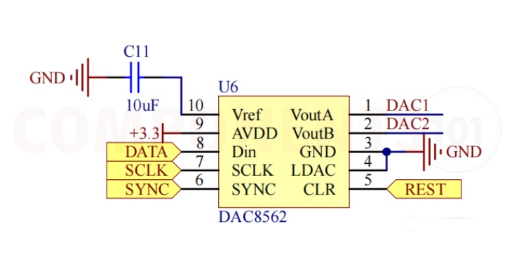
To connect the DAC8562, you'll need to establish several connections. Firstly, ensure proper power supply within the specified voltage range of 2.7V to 5.5V. Connect SPI lines such as SCLK, MOSI, and MISO from your microcontroller to the corresponding pins on the DAC8562. Additionally, link the chip select (CS) pin to enable communication between the microcontroller and the DAC. Set up a reference voltage source and connect it to the REF pin of the DAC to establish the desired output range. Ensure proper grounding by connecting the GND pin of the DAC8562 to the ground of your system. You can use the same connection for the DAC8562 Arduino interface too. You can use dedicated libraries like this DAC8562 library to communicate with our DAC IC.
DAC8562 Troubleshooting Guide:
Does the DAC8562 interfere with EMF signals?
Yes, the DAC8562 will interfere with EMF lines so Consider using shielding techniques to protect the DAC from external electromagnetic interference.
My DAC8562 is not providing any output. What could be the issue?
First, ensure that the power supply voltages are within the specified range (2.7V to 5.5V). Check the connections to the DAC8562, including AVDD, GND, and the reference voltage.
I'm experiencing erratic output from the DAC8562. What might be causing this?
Erratic output can be due to noise or interference in the system. Ensure that the analog input signal is adequately filtered and shielded from noise sources. Verify that the ground connections are solid and free from ground loops. Additionally, check the integrity of the clock signal (CLK) and ensure that it meets the DAC8562 timing requirements.
How to reduce the noise while using DAC8562?
Ensure proper decoupling capacitors are placed close to the DAC to filter out high-frequency noise on the power supply lines.Use a solid ground plane and connect it directly to the DAC's ground pin. Avoid ground loops and minimize the length of high-current ground paths.
Things to Consider When Using DAC8562 in Your Design:
When designing with the DAC8562, a 12-bit Digital-to-Analog Converter (DAC), here are some important considerations and design tips to keep in mind:
Layout Guidelines
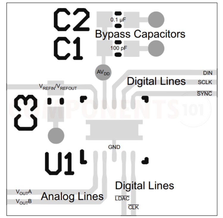
A precision analog component requires careful layout, adequate bypassing, and clean, well-regulated power supplies. The DAC756x, DAC816x, and DAC856x devices offer single-supply operation and are often used in close proximity with digital logic, microcontrollers, microprocessors, and digital signal processors. The more digital logic presents in the design and the higher the switching speed, the more difficult it is to keep digital noise from appearing at the output. As a result of the single ground pin of the DAC756x, DAC816x, and DAC856x devices, all return currents (including digital and analog return currents for the DAC) must flow through a single point. Ideally, GND would be connected directly to an analog ground plane. This plane would be separate from the ground connection for the digital components until they were connected at the power-entry point of the system. The power applied to AVDD should be well-regulated and low noise. Switching power supplies and DC-DC converters often have high-frequency glitches or spikes riding on the output voltage. In addition, digital components can create similar high-frequency spikes as their internal logic switches states. This noise can easily couple into the DAC output voltage through various paths between the power connections and analog output. As with the GND connection, AVDD should be connected to a power-supply plane or trace that is separate from the connection for digital logic until they are connected at the power-entry point. In addition, a pair of 100-pF to 1-nF capacitors and a 0.1-µF to 1-µF bypass capacitor are strongly recommended. In some situations, additional bypassing may be required, such as a 100-µF electrolytic capacitor or even a pi filter made up of inductors and capacitors – all designed essentially to provide low-pass filtering for the supply and remove the high-frequency noise.
Power Supply Recommendations
This device can operate within the specified supply voltage range of 2.7 V to 5.5 V. The power applied to AVDD should be well-regulated and low-noise. In order to further minimize noise from the power supplies, a strong recommendation is to include a pair of 100-pF and 1-nF capacitors and a 0.1-μF to 1-μF bypass capacitor.
Applications of DAC8562
- Portable Instrumentation
- PLC Analog Output Module
- Closed-Loop Servo Control
- Voltage Controlled Oscillator Tuning
- Data Acquisition Systems
- Programmable Gain and Offset Adjustment
How to Order DAC8562?
As we discussed the DAC8562 is available in two different packages VSSOP and WSON. The VSSOP package chips are available in the following part numbers: DAC8562SDGSR, DAC8562SDGST and the WSON packaged chips are available in the following part numbers: DAC8562SDSCR, DAC8562SDSCT. Other than the different chip packages all these are the same. The only difference between these two types is the number of chips per ordering package.
2D Model and Dimensions of DAC8562
Here you can find the mechanical drawings of DAC8562 along with its dimensions. The dimensions can be used to create custom footprints of the module and be used for PCB or CAD modeling.