DAC0808 – 8 Bit D/A Converter
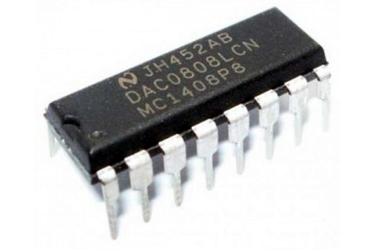
DAC0808 is a D/A converter IC and is used for converting 8-bit digital data input to analog signal output. It is a monolithic IC featuring a full scale output current settling time of 150 ns while dissipating only 33 mW with ±5V supplies. The chip accuracy of conversion is good and power consumption is also low to make it popular. The power supply currents of the DAC0808 are independent of bit codes, and exhibits essentially constant device characteristics over the entire supply voltage range.
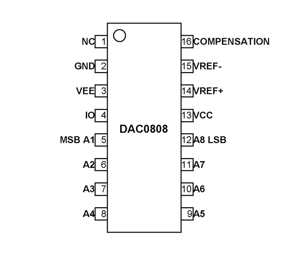
DAC0808 Pinout Configuration
DAC0808 is a sixteen pin device and description for each pin is given below:
|
Pin |
Name |
Description |
|
1 |
NC |
No connection |
|
2 |
GND |
Ground |
|
3 |
VEE |
Negative power supply |
|
4 |
IO |
Output signal pin |
|
5 |
A1 |
Digital input bit 1 (Most Significant Bit) |
|
6 |
A2 |
Digital input bit 2 |
|
7 |
A3 |
Digital input bit 3 |
|
8 |
A4 |
Digital input bit 4 |
|
9 |
A5 |
Digital input bit 5 |
|
10 |
A6 |
Digital input bit 6 |
|
11 |
A7 |
Digital input bit 7 |
|
12 |
A8 |
Digital input bit 8 (Least Significant Bit) |
|
13 |
VCC |
Positive power supply |
|
14 |
VREF+ |
Positive reference voltage |
|
15 |
VREF- |
Negative reference voltage |
|
16 |
COMPENSATION |
Compensation capacitor pin |
Features and Electrical Characteristics
- 8 bit parallel digital data input
- Fast settling time (typical value): 150 ns
- Relative accuracy at ±0.19% maximum error
- Full scale current match: ±1 LSB
- Non-inverting digital inputs are TTL and CMOS compatible
- High speed multiplying input slew rate: 8 mA/μs
- Power supply voltage range: ±4.5V to ±18V
- Low power consumption: 33 mW@ ±5V
- Maximum Power dissipation: 1000 mW
- Operating temperature range: 0ºC to +75ºC
Note: Complete technical information can be found in the DAC0808 Datasheet, linked at the bottom of this page.
Similar D/A Converters
DAC0807, DAC0806, DAC0800, DAC0802, AD557
Overview of DAC0808
DAC0808 IC is used in applications where a digital-to-analog conversion is required. The chip used to be popular a decade ago and its applications used to be many, but at present, there are many modern ICs that can perform DAC with higher resolution, speed, and efficiency. So this device is mainly used for reference and beginner applications and nothing more. For advanced applications, a microcontroller with DAC feature or DAC IC with the serial interface is preferred at present.
How to use DAC0808 IC
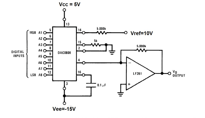
A typical application circuit for DAC0808 is already given in the datasheet and we can use that circuit to develop applications without worry as the circuit is tested working.
In circuit
- For the working of device DAC0808, we need two voltage sources +5V and -15V as shown in the diagram. This is a major drawback that is eliminated in modern DAC to make them work from a single power source.
- Eight digital inputs are given to the chip and are supposed to be in order from MSB to LSB. This is also a major drawback because we need to waste 8 I/O pins. This is also eliminated in modern DACs.
- A +10V power source is connected as a reference voltage for the device and the negative reference is grounded.
Working
The device takes in parallel 8-bit data from a microcontroller or microprocessor and converts that data into an analog signal at the output. And the analog output from DAC is a current quantity, and this needs to be converted into voltage parameters for use in application easily. So to convert the current parameter into voltage parameter, we will use an op-amp circuit as shown in the circuit diagram. This op-amp circuit is called current-to-voltage converter.
The output analog voltage from op-amp is in linear relation with input digital value and hence DAC conversion with DAC0808 is achieved. Similarly, you can also use other application circuits for DAC0808 given in the datasheet.
Applications
- Analog and digital circuits
- Electrical measurements
- Audio conversion
- Hobbyist applications
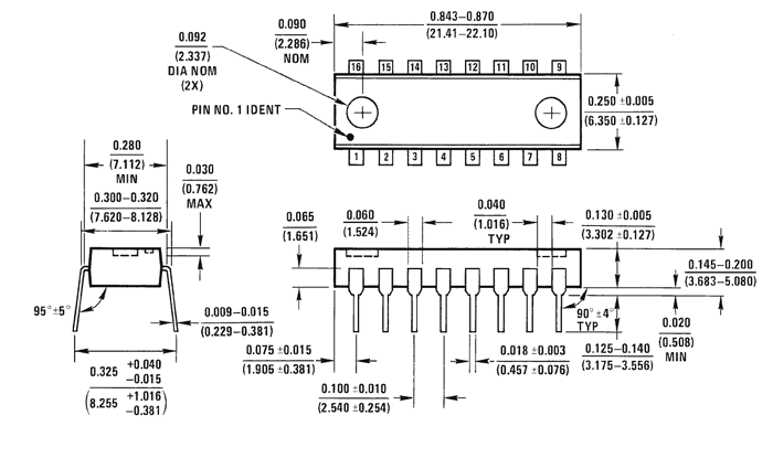
2D-Model and Dimensions
All dimensions are in inches [millimeter measurements in brackets]
