AD5737 16-Bit, Low-Power, Buffered Output, Rail-to-Rail DAC

The AD5737 is a quad-channel current output digital-to-analog converter (DAC) from Analog Devices. This DAC offers four independently programmable output channels, each capable of providing a current output. In addition, each channel of the AD5737 includes a corresponding CHART pin, which allows HART signals to be coupled to the current output of the AD5737. This feature is useful in applications where HART communication is required. It has an input power supply range from 10.8 V to 33 V. The AD5737 includes on-chip dynamic power control, which is used to minimize package power dissipation. This is achieved by regulating the voltage on the output driver within a range of 7.4 V to 29.5 V. The AD5737's versatile interface makes it compatible with a wide range of communication standards like SPI, QSPI, MICROWIRE, DSP etc. which can be very convenient for various system integration needs. It is commonly used in applications where precise current control is required, such as in industrial automation, instrumentation, and control systems.
AD5737 Pinout Configuration
Here are the pinout details for AD5737.
| Pin Number | Name | Function |
| 1 | RSET_B | External Current Setting Resistor section. |
| 2 | RSET_A | External Current Setting Resistor section. |
| 3 | REFGND | Ground Reference Point for Internal Reference. |
| 4 | REFGND | Ground Reference Point for Internal Reference. |
| 5 | AD0 | Address Decode for the Device Under Test (DUT) on the Board. |
| 6 | AD1 | Address Decode for the DUT on the Board. |
| 7 | SYNC | Frame Synchronization Signal for the Serial Interface |
| 8 | SCLK | Serial Clock Input |
| 9 | SDIN | Serial Data Input. |
| 10 | SDO | Serial Data Output. |
| 11 | DVDD | Digital Supply Pin. |
| 12 | DGND | Digital Ground. |
| 13 | LDAC | Load DAC |
| 14 | CLEAR | CLEAR |
| 15 | ALERT | Alert |
| 16 | FAULT | Active Low, Open-Drain Output. |
| 17 | DGND | Digital Ground. |
| 18 | RESET | Hardware Reset |
| 19 | AVDD | Positive Analog Supply Pin. |
| 20 | NC | No Connect. |
| 21 | CHARTA | HART Input Connection |
| 22 | IGATEA | Optional Connection for External Pass Transistor. |
| 23 | COMPDCDC_A | DC-to-DC Compensation Capacitor.. |
| 24 | VBOOST_A | Supply for Channel A Current Output Stage. |
| 25 | NC | No Connect. |
| 26 | IOUT_A | Current Output Pin for DAC Channel A. |
| 27 | AGND | Ground Reference Point for Analog Circuitry. |
| 28 | NC | No Connect. Do not connect to this pin. |
| 29 | CHARTB | HART Input Connection for DAC Channel B. For more information, see the HART Connectivity section. |
| 30 | NC | No Connect. Do not connect to this pin. |
| 31 | IGATEB | Optional Connection for External Pass Transistor. |
| 32 | COMPDCDC_B | DC-to-DC Compensation Capacitor. Connect a 10 nF capacitor from this pin to ground. |
| 33 | IOUT_B | Current Output Pin for DAC Channel B. |
| 34 | VBOOST_B | Supply for Channel B Current Output Stage |
| 35 | AGND | Ground Reference Point for Analog Circuitry. This pin must be connected to 0 V. |
| 36 | SWB | Switching Output for Channel B DC-to-DC Circuitry. |
| 37 | GNDSWB | Ground Connection for DC-to-DC Switching Circuit. This pin must always be connected to ground. |
| 38 | GNDSWA | Ground Connection for DC-to-DC Switching Circuit. This pin must always be connected to ground. |
| 39 | SWA | Switching Output for Channel A DC-to-DC Circuitry. |
| 40 | AGND | Ground Reference Point for Analog Circuitry. This pin must be connected to 0 V. |
| 41 | SWD | Switching Output for Channel D DC-to-DC Circuitry |
| 42 | GNDSWD | Ground Connection for DC-to-DC Switching Circuit. This pin must always be connected to ground. |
| 43 | GNDSWC | Ground Connection for DC-to-DC Switching Circuit. This pin must always be connected to ground. |
| 44 | SWC | Switching Output for Channel C DC-to-DC Circuitry. |
| 45 | AVCC | Supply for DC-to-DC Circuitry. The voltage range is from 4.5 V to 5.5 V. |
| 46 | VBOOST_C | Supply for Channel C Current Output Stage |
| 47 | IOUT_C | Current Output Pin for DAC Channel C. |
| 48 | COMPDCDC_C | DC-to-DC Compensation Capacitor. |
| 49 | IGATEC | Optional Connection for External Pass Transistor. |
| 50 | NC | No Connect. |
| 51 | CHARTC | HART Input Connection for DAC Channel C. |
| 52 | NC | No Connect. |
| 53 | AGND | Ground Reference Point for Analog Circuitry. |
| 54 | IOUT_D | Current Output Pin for DAC Channel D. |
| 55 | NC | No Connect. |
| 56 | VBOOST_D | Supply for Channel D Current Output Stage. |
| 57 | COMPDCDC_D | DC-to-DC Compensation Capacitor. |
| 58 | IGATED | Optional Connection for External Pass Transistor |
| 59 | CHARTD | HART Input Connection for DAC Channel D. |
| 60 | NC | No Connect. Do not connect to this pin. |
| 61 | REFIN | External Reference Voltage Input. |
| 62 | REFOUT | Internal Reference Voltage Output. |
| 63 | RSET_D | An external, precision, low drift, 15 kΩ current setting resistor can be connected to this pin to improve the IOUT_D temperature drift performance. For more information, see the External Current Setting Resistor section. |
| 64 | RSET_C | An external, precision, low drift, 15 kΩ current setting resistor can be connected to this pin to improve the IOUT_C temperature drift performance. For more information, see the External Current Setting Resistor section. |
Features of AD5737
AD5737 ADC chip has the following key features:
- 12-bit resolution and monotonicity
- Dynamic power control for thermal management or external PMOS mode
- Current output ranges: 0 mA to 20 mA, 4 mA to 20 mA,
- and 0 mA to 24 mA
- ±0.1% total unadjusted error (TUE) maximum User-programmable offset and gain
- On-chip diagnostics
- On-chip reference: ±10 ppm/°C maximum
- −40°C to +105°C temperature range
Manufacturers of AD5737:
The AD5737 is manufactured by Analog Devices (earlier this IC was from Maxim Integrated). There are no alternative manufacturers for the same part number as of the date of writing this article.
AD5737 Equivalents
There is no pin-to-pin compatible equivalent for AD5737 we could find at the time of writing this.
AD5737 Alternatives
If you are looking for an alternative for AD5737 you can look at the other IC from these.
DAC8562, MCP4725, MCP4921, PT8211, DAC0832, DAC0808, DAC7715, AD5421
Note: Complete technical details can be found in the AD5737 datasheet at this page’s end.
AD5737 Circuit Diagram
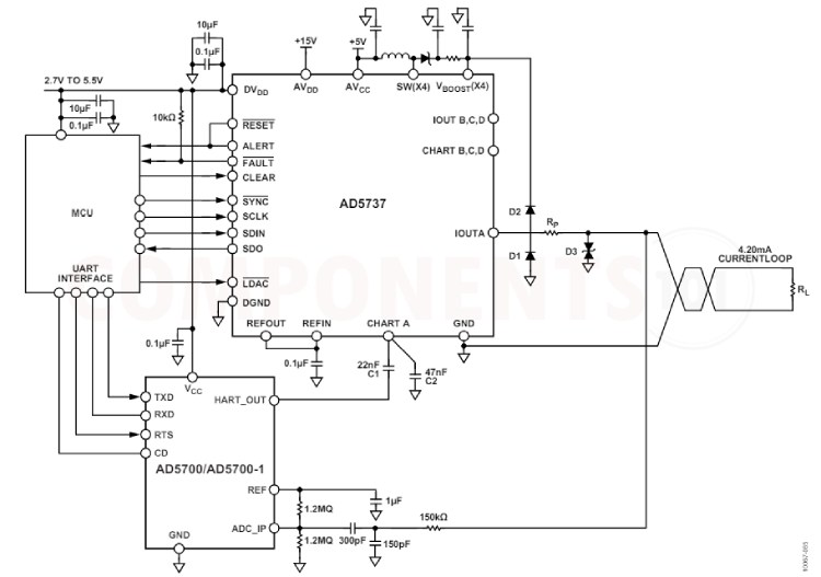
The above image shows the AD5737 in a circuit design for a HART-enabled output module, specifically for use in an industrial control application.
The design provides for a HART-enabled current output, with the HART capability provided by the AD5700/AD5700-1 HART modem, the industry’s lowest power and smallest footprint HART-compliant IC modem. For additional space savings, the AD5700-1 offers a 0.5% precision internal oscillator. The HART_OUT signal from the AD5700 is attenuated and ac-coupled into the CHARTx pin of the AD5737. Such a configuration results in the AD5700 HART modem output modulating the 4 mA to 20 mA analog current without affecting the dc level of the current. This circuit adheres to the HART physical layer specifications as defined by the HART Communication Foundation. For transient overvoltage protection, a 24 V transient voltage suppressor (TVS) is placed on the IOUT/VOUT connection. For added protection, clamping diodes are connected from the IOUT_x/VOUT_x pin to the AVDD and GND power supply pins. A 5 kΩ current limiting resistor is also placed in series with the +VSENSE_x input. This is to limit the current to an acceptable level during a transient event. The recommended external band-pass filter for the AD5700 HART modem includes a 150 kΩ resistor, which limits current to a sufficiently low level to adhere to intrinsic safety requirements. In this case, the input has higher transient voltage protection and, therefore, does not require additional protection circuitry, even in the most demanding of industrial environments.
AD5737 Troubleshooting Guide
My AD5737 is not providing any output. What could be the issue?
First, ensure that the power supply voltages are within the specified range (10.8 V to 33 V). Check the connections to the AD5737, including VDD, GND, and the reference voltage.
My circuits show a lot of noise, how to reduce it?
Should use bypass capacitors in between VDD and GND. Use a solid ground plane and connect it directly to the DAC's ground pin. Avoid ground loops and minimize the length of high-current ground paths.
Does the AD5737 interfere with EMF signals?
Yes, the AD5737 will interfere with EMF lines so Consider using shielding techniques to protect the DAC from external electromagnetic interference.
Things to Consider When Using AD5737 in Your Design
When designing with the AD5737, digital-analog Converter (ADC), here are some important considerations and design tips to keep in mind:
Microprocessor Interfacing
Microprocessor interfacing to the AD5737 is via a serial bus that uses a protocol compatible with microcontrollers and DSP processors. The communication channel is a 3-wire minimum interface consisting of a clock signal, a data signal, and a latch signal. The AD5737 requires a 24-bit data-word with data valid on the falling edge of SCLK. The DAC output update is initiated either on the rising edge of LDAC or, if LDAC is held low, on the rising edge of SYNC. The contents of the registers can be read using the readback function.
Traces
The power supply lines of the AD5737 must use as large a trace as possible to provide low impedance paths and reduce the effects of glitches on the power supply line. Fast-switching signals such as clocks must be shielded with digital ground to prevent radiating noise to other parts of the board and must never be run near the reference inputs. A ground line routed between the SDIN and SCLK traces helps reduce crosstalk between them (not required on a multilayer board that has a separate ground plane, but separating the lines helps). It is essential to minimize noise on the REFIN line because it couples through to the DAC output.
Avoid crossover of digital and analog signals. Traces on opposite sides of the board must run at right angles to each other.
to reduce the effects of feedthrough on the board. A microstrip technique is by far the best method, but it is not always possible with a double-sided board. In this technique, the component side of the board is dedicated to the ground plane, and signal traces are placed on the solder side.
DC-to-DC Converters
To achieve high efficiency, good regulation, and stability, a well-designed printed circuit board layout is required.
Follow these guidelines when designing printed circuit boards.
- Keep the low ESR input capacitor, CIN, close to AVCC and PGND.
- Keep the high current path from CIN through the inductor (LDCDC) to SWx and PGND as short as possible.
- Keep the high current path from CIN through the inductor (LDCDC), the diode (DDCDC), and the output capacitor (CDCDC) as short as possible.
- Keep high current traces as short and as wide as possible. The path from CIN through the inductor (LDCDC) to SWx and PGND must be able to handle a minimum of 1 A.
- Place the compensation components as close as possible to the COMPDCDC_x pin.
- Avoid routing high impedance traces near any node connected to SWx or near the inductor to prevent radiated noise injection.
Layout Guidelines
Grounding- In any circuit where accuracy is important, careful consideration of the power supply and ground return layout helps to ensure the rated performance. The printed circuit board on which the AD5737 is mounted must be designed so that the analog and digital sections are separated and confined to certain areas of the board. If the AD5737 is in a system where multiple devices require an AGND-to-DGND connection, the connection must be made at one point only. The star ground point must be established as close as possible to the device. The GNDSWx pin and the ground connection for the AVCC supply are referred to as PGND. PGND must be confined to certain areas of the board, and the PGND-to-AGND connection must be made at one point only.
Supply Decoupling- The AD5737 must have ample supply bypassing of 10 μF in parallel with 0.1 μF on each supply, located as close to the package as possible, ideally right up against the device. The 10 μF capacitors are the tantalum bead type. The 0.1 μF capacitors must have low effective series resistance (ESR) and low effective series inductance (ESL), such as the common ceramic types, which provide a low impedance path to ground at high frequencies to handle transient currents due to internal logic switching.
Applications of AD5737
- Process control
- Actuator control
- PLCs
- HART network connectivity
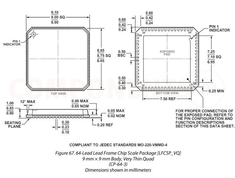
AD5737 Footprint Information
Here you can find the mechanical drawings of AD5737 along with its dimensions. The dimensions can be used to create custom footprints of the module and be used for PCB or CAD modeling.