AD5421-16-Bit, Serial Input, Loop-Powered DAC
The AD5421 is a complete, high precision, fully integrated, low-cost, loop-powered, 4 mA to 20 mA Digital-to-Analog converter (DAC). This DAC is designed for use in industrial control applications, particularly in smart transmitters. The AD5421 includes an integrated voltage regulator that provides a regulated output voltage, typically ranging from 1.8 V to 12 V. This regulated voltage output can be used to power the AD5421 itself, as well as other devices in the transmitter circuit. The AD5421 is designed to be compatible with the Highway Addressable Remote Transducer (HART) communication protocol, specifically the Frequency Shift Keying (FSK) modulation used in HART communication. This compatibility allows the AD5421 to be used in applications where HART communication is required. This DAC comes with a serial interface and is capable of operating at 30 MHz and allows for simple connection to commonly used microprocessors and microcontrollers via a SPI-compatible, 3-wire interface. The AD5421 is guaranteed to be monotonic to 16 bits, ensuring that the output of the DAC increases or decreases monotonically with increasing digital input code. This IC is available in 28-lead TSSOP and 32-lead LFCSP Packages.
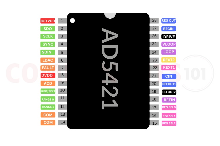
AD5421 Pinout Configuration
Here are the pinout details for AD5421.
| Pin Number | Name | Function |
| 1 | IODVDD | Digital Interface Supply Pin |
| 2 | SDO | Serial Data Output. |
| 3 | SCLK | Serial Clock Input. |
| 4 | SYNC | Frame Synchronization Input |
| 5 | SDIN | Serial Data Input |
| 6 | LDAC | Load DAC InpuT |
| 7 | FAULT | Fault Alert Output Pin |
| 8 | DVDD | 3.3 V Digital Power Supply Output. |
| 9 | ALARM_ CURRENT_ DIRECTION | Alarm Current Direction Select. |
| 10 | RINT/REXT | Current Setting Resistor Select. |
| 11 | RANGE0 | Digital Input Pins. |
| 12 | RANGE1 | Digital Input Pins. |
| 13 | COM | Ground Reference Pin |
| 14 | COM | Ground Reference Pin |
| 15 | REG_SEL2 | regulator output (REGOUT) voltage |
| 16 | REG_SEL1 | regulator output (REGOUT) voltage |
| 17 | REG_SEL0 | regulator output (REGOUT) voltage |
| 18 | REFIN | Reference Voltage Input. |
| 19 | REFOUT2 | Internal Reference Voltage Output |
| 20 | REFOUT1 | Internal Reference Voltage Output |
| 21 | CIN | External Capacitor Connection and HART FSK Input |
| 22 | REXT1 | Connection for External Current Setting Resistor |
| 23 | REXT2 | Connection for External Current Setting Resistor |
| 24 | LOOP | Loop Current Return Pin |
| 25 | VLOOP | Voltage Input Pin |
| 26 | DRIVE | Gate Connection for External Depletion Mode MOSFET |
| 27 | REGIN | Voltage Regulator Input. |
| 28 | REGOUT | Voltage Regulator Output |
Features of AD5421
AD5421 ADC chip has the following key features:
- 16-bit resolution and monotonicity
- Pin selectable NAMUR-compliant ranges (4 mA to 20 mA, 3.8 mA to 21 mA,3.2 mA to 24 mA)
- NAMUR-compliant alarm currents(Downscale alarm current = 3.2 mA Upscale alarm current = 22.8 mA/24 mA)
- Total unadjusted error (TUE): 0.05% maximum
- INL error: 0.0035% FSR maximum
- Output TC: 3 ppm/°C typical
- Quiescent current: 300 μA maximum
- Flexible SPI-compatible serial digital interface with Schmitt triggered inputs
- On-chip fault alerts via FAULT pin or alarm current
- Automatic readback of fault register on each write cycle
- Slew rate control function
- Gain and offset adjust registers
- On-chip reference TC: 4 ppm/°C maximum
- Selectable regulated voltage output
- Loop voltage range: 5.5 V to 52 V
- Temperature range: −40°C to +105°C
- TSSOP and LFCSP packages
Manufacturers of AD5421:
The AD5421 is manufactured by Analog Devices. There are no alternative manufacturers for the same part number as of the date of writing this article.
AD5421 Equivalents
There is no equivalent replacement for AD5421.
AD5421 Alternatives
If you are looking for an alternative for AD5421 you can look at the other IC from these.
DAC8562, MCP4725, MCP4921, PT8211, DAC0832, DAC0808, DAC7715, AD5737, MAX5216, MCP4922
Note: Complete technical details can be found in the AD5421 datasheet at this page’s end.
AD5421 Typical Circuit Diagram
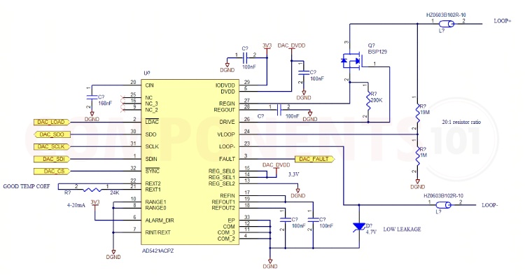
The above diagram shows a typical AD5421 Application Diagram To reduce power dissipation on the chip, a depletion mode MOSFET (Q1), such as a DN2540 or BSP129, can be connected between the loop voltage and the AD5421, as shown. If a low loop voltage is used, T1 does not need to be inserted, and the loop voltage can connect directly to REGIN. All interface signal lines are connected to the microcontroller. To reduce the number of interface signal lines, the LDAC signal can be connected to COM, and the SDO and FAULT lines can be left unconnected. However, this configuration disables the use of the fault alert features. Under normal operating conditions, the voltage between COM and LOOP− does not exceed 1.5 V, and the voltage at LOOP− is negative with respect to COM. If it is possible that the voltage at LOOP− may be forced positive with respect to COM, or if the voltage difference between LOOP− and COM may be forced in excess of 5 V, a 4.7 V low leakage Zener diode should be placed between COM and the LOOP− pin, as shown in Figure 50, to protect the AD5421 from potential damage.
AD5421 Troubleshooting Guide
AD5421 is not providing any output. What could be the issue?
First, ensure that the power supply voltages are within the specified range. (2.7V to 5.5V). Check the connections to the AD5421, including IODVDD, DVDD, and the COM.
AD5421 circuit shows a lot of noise, how to reduce it?
Should use bypass capacitors in between IODVDD and COM. Use a solid ground plane and connect it directly to the DAC's ground pin. Avoid ground loops and minimize the length of high-current ground paths.
Does the AD5421 interfere with EMF signals?
Yes, the AD5421 will interfere with EMF lines so Consider using shielding techniques to protect the DAC from external electromagnetic interference.
Is there an evaluation board available for AD5421?
Yes, there is an evaluation board for AD5421 available from ANalog Devices. You can check out the part number EVAL-AD5421SDZ.
How to do AD5421 Arduino interfacing?
The AD5421 uses a standard SPI protocol for communication. So, you can use the SPI bus available in the Arduino to communicate with the AD5421. More details about the SPI communication can be found in the datasheet.
Things to Consider during AD5421 ADC Design
When designing with the AD5421, a 16-bit Analog-to-Digital Converter (ADC), here are some important considerations and design tips to keep in mind:
Thermal and supply considerations
The AD5421 is designed to operate at a maximum junction temperature of 125°C. To ensure reliable and specified operation over the lifetime of the product, it is important that the device not be operated under conditions that cause the junction temperature to exceed this value.
Maximum Power Dissipation
Maximum permitted power dissipation when operating at an ambient temperature of 105°C.
Maximum Ambient Temperature
Maximum permitted ambient temperature when operating from a supply of 52 V while regulating a loop current of 22.8 mA.
Maximum Supply Voltage
Maximum permitted supply voltage when operating at an ambient temperature of 105°C while regulating a loop current of 22.8 mA.
Applications of AD5421
- Industrial process control
- loop-powered transmitters.
- Smart transmitters
- HART network connectivity
MCP4922 Ordering Information
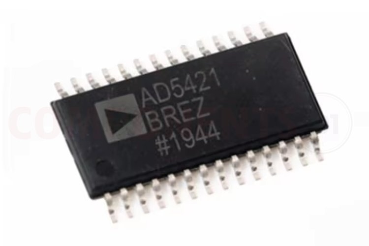
AD5421BREZ, AD5421BREZ-REEL, AD5421BREZ-REEL7, AD5421CREZ, AD5421CREZ-RL and AD5421CREZ-RL7 come in 28-pin TSSOP package while the AD5421ACPZ-REEL7 and AD5421BCPZ-REEL7 come in 32 pin LFCP Package.
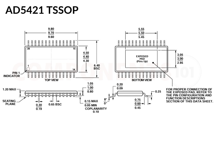
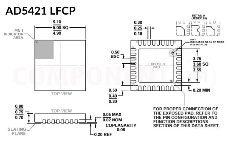
AD5421 Footprint Information
Here you can find the mechanical drawings of AD5421 along with its dimensions. The dimensions can be used to create custom footprints of the module and be used for PCB or CAD modelling.