

Optimized with highly sensitive cap touch sensors, extensive peripheral circuits and 125℃ operation
Boost Converter: Basics, Working, Design & Operation
We’ve all come across pesky situations where we need a slightly higher voltage than our power supplies can provide. We need 12 volts but have only a 9-volt battery. Or maybe we have a 3.3V supply when our chip needs 5V. That too, in most cases, the current draw is quite decent.
Eventually, we ask ourselves the question, is it possible to convert one DC voltage to another?
Lucky for us, the answer is yes. It is possible to convert one DC voltage to another, however, the methods are slightly on the clever side.
And no, it does not involve the conversion of DC to AC and back again. As it involves too many steps. Anything that has too many steps is inefficient; this is a good life lesson too.
Enter the world of switch mode DC-DC converters!
They’re called switch mode because there’s usually a semiconductor switch that turns on and off very rapidly.
What is a Boost Converter?
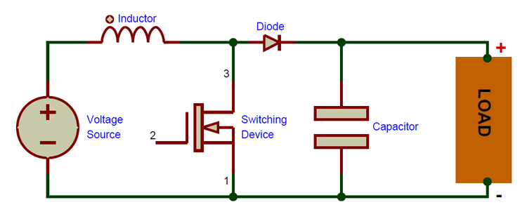
A boost converter is one of the simplest types of switch mode converter. As the name suggests, it takes an input voltage and boosts or increases it. All it consists of is an inductor, a semiconductor switch (these days it’s a MOSFET, since you can get really nice ones these days), a diode, and a capacitor. Also needed is a source of a periodic square wave. This can be something as simple as a 555 timer or even a dedicated SMPS IC like the famous MC34063A IC.
As you can see, there are only a few parts required to make a boost converter. It is less cumbersome than an AC transformer or inductor.
They’re so simple because they were originally developed in the 1960s to power the electronics systems on aircraft. It was a requirement that these converters be as compact and as efficient as possible.
The biggest advantage boost converters offer is their high efficiency – some of them can even go up to 99%! In other words, 99% of the input energy is converted to useful output energy, only 1% is wasted.
How Does a Boost Converter Work?
It’s time to take a really deep breath, we’re about to plunge into the depths of power electronics. I’ll say at the outset that it is a very rewarding field.
To understand the working of a boost converter, it is mandatory that you know how inductors, MOSFETs, diodes and capacitors work.
With that knowledge, we can go through the working of the boost converter step by step.
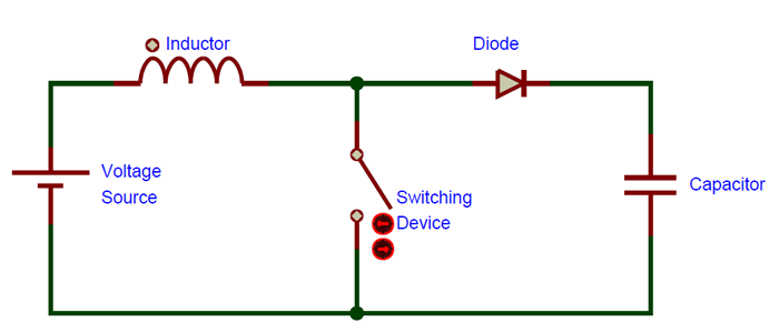
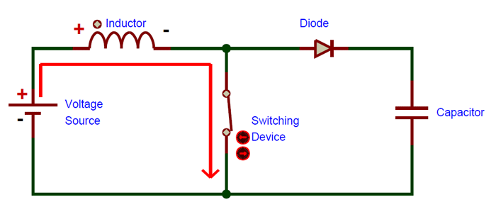
STEP – 1
Here, nothing happens. The output capacitor is charged to the input voltage minus one diode drop.
STEP – 2
Now, it’s time to turn the switch on. Our signal source goes high, turning on the MOSFET. All the current is diverted through to the MOSFET through the inductor. Note that the output capacitor stays charged since it can’t discharge through the now back-biased diode.
The power source isn’t immediately short circuited, of course, since the inductor makes the current ramp up relatively slowly. Also, a magnetic field builds up around the inductor. Note the polarity of the voltage applied across the inductor.
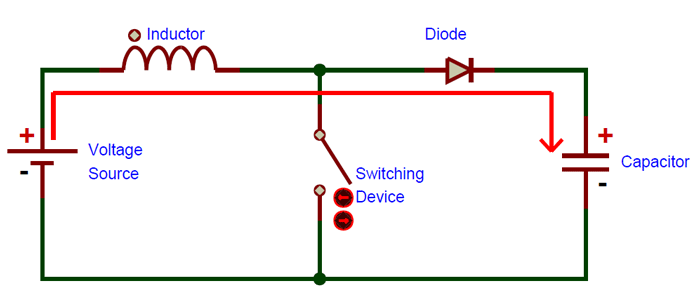
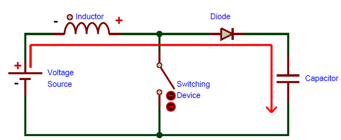
STEP – 3
The MOSFET is turned off and the current to the inductor is stopped abruptly.
The very nature of an inductor is to maintain smooth current flow; it doesn’t like sudden changes in current. So it does not like the sudden turning off of the current. It responds to this by generating a large voltage with the opposite polarity of the voltage originally supplied to it using the energy stored in the magnetic field to maintain that current flow.
If we forget the rest of the circuit elements and notice only the polarity symbols, we notice that the inductor now acts like a voltage source in series with the supply voltage. This means that the anode of the diode is now at a higher voltage than the cathode (remember, the cap was already charged to supply voltage in the beginning) and is forward biased.
The output capacitor is now charged to a higher voltage than before, which means that we have successfully stepped up a low DC voltage to a higher one!
I recommend that you go through the steps once again very slowly and understand them intuitively.
These steps happen many thousands of times (depending on the frequency of the oscillator) to maintain the output voltage under load.
Boost Converter Operation - The Fine Points
By now many of you already have questions about this oversimplified explanation. There was a lot left out, but it was worth it to make the working of the boost converter absolutely clear. So now that we have that understanding, we can move on to the finer details.
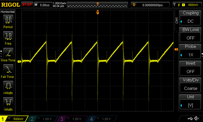
1. The Oscillator. You can’t keep the MOSFET output switch on forever, no inductor is ideal – they have saturation currents. If we did keep the MOSFET switch on for any longer than a few hundred microseconds max, the supply will be short circuited and the inductor insulation burns off and the MOSFET goes bust and other nasty things happen. We use our knowledge of inductors to calculate the time required to reach a sensible current (one Amp, for example) and then configure the on time of the oscillator accordingly. This results in the inductor current waveform looking like a saw edge, hence the name sawtooth.
2. The MOSFET itself. If you look closely, during step 3, the MOSFET sees a voltage that is the supply voltage plus the inductor voltage, which means that the MOSFET has to be rated for a high voltage, which again implies a rather high on resistance. Boost converter design is always a compromise between MOSFET breakdown voltage and on resistance. The switching MOSFET of the boost converter is always the weak point, as I learned from cold, hard experience. The maximum output voltage of the boost converter is not limited by design but by the breakdown voltage of the MOSFET.
3. The inductor. Obviously, just any old inductor won’t work. Inductors used in boost converters should be able to withstand the high currents and have a highly permeable core, so that the inductance for a given size is high.
Boost Converter Operation
There is yet another way of thinking about the operation of a boost converter.
We know that the energy stored in an inductor is given by:
½ x L x I2
Where L is the inductance of the coil and I is the maximum peak current.
So we store some energy in the inductor from the input and transfer that same energy to the output though at a higher voltage (power is conserved, obviously). This happens many thousands of times a second (depending on the oscillator frequency) and so the energy adds up in every cycle so you get a nice measurable and useful energy output, for example 10 Joules every second, i.e. 10 watts.
As the equation tells us, the energy stored in the inductor is proportional to the inductance and also to the square of the peak current.
To increase output power, our first thought might be to increase the size of the inductor. Of course, this will help, but not as much as we think! If we make the inductance larger, the maximum peak current that can be achieved in a given time decreases, or the time taken to reach that current increases (remember the basic equation V/L = dI/dt), so the overall output energy does not increase by a significant amount!
However, since energy is proportional to the square of the maximum current, increasing the current will lead to a larger increase in output energy!
So we understand that choosing the inductor is a fine balance between inductance and peak current.
With this knowledge we can being to understand the formal method of designing a boost converter.
Boost Converter Design
STEP – 1
To begin with, we need a thorough understanding of what our load requires. It is highly recommended (from experience) that if you attempt to build a boost converter at the beginning it is very important to know the output voltage and current independently, the product of which is our output power.
STEP – 2
Once we have the output power, we can divide that by the input voltage (which should also be decided) to get the average input current needed.
We increase the input current by 40% to account for ripple. This new value is the peak input current.
Also the minimum input current is 0.8 times the average input current, so multiply the average input current by 0.8.
Now that we have peak and minimum current, we can calculate the total change in current by subtracting the peak and minimum current.
STEP – 3
Now we calculate the duty cycle of the converter, i.e. the ratio of the on and off times of the oscillator.
Duty cycle is given by this textbook formula:
D.C. = (Vout – Vin)/(Vout)
This should give us a reasonable decimal value, above 0 but below 0.999.
STEP – 4
Now it is time to decide upon the frequency of the oscillator. This has been included as a separate step because the signal source can be anything from a 555 timer (where the frequency and duty cycle are completely under your control) or a fixed frequency PWM controller.
Once the frequency is determined, we can find out the total time period by taking an inverse.
Now the time period is multiplied by the duty cycle value to get the on time.
STEP – 5
Since we have determined the on time, input voltage and change in current, we can plug those values into the inductor formula which has been rearranged a little:
L = (V*dt)/dI
Where V is the input voltage, dt is the on time and dI is the change in current.
Don’t worry if the inductor value is not a commonly available one, use the closest standard value available. With a little tweaking, the system should work just fine.
Selection of Parts
1. Switching Transistor
I’ve not mentioned the type since that is completely based on the application. Of course, the MOSFET is used in all applications these days, since they are very efficient, but there may be situations where a normal bipolar transistor may suffice because of simplicity.
I’ll repeat what I’ve said before – pick a transistor with a breakdown voltage that is higher than the maximum output voltage of the converter.
It might also be a good choice to look at the MOSFET datasheet and determine the input capacitance/gate capacitance. The lower this value is, the easier the driving requirements are. Anything below 3500pF is acceptable and moderately easy to drive.
My personal choice would be the IRF3205, which has an on resistance of 8 milliOhms and a breakdown voltage of 55V, with a manageable input capacitance of 3247pF, besides being an easily available part.
Also not mentioned in the schematic was a dedicated MOSFET gate driver. Again, I *highly* recommend using one. It’ll save you a lot of losses and time. My recommendation – the TC4427. It has two drivers in one DIP8 package, which can be paralleled easily for more drive current.
2. Output Diode
Though this may seem trivial, at the currents we are dealing with (or sometimes voltage) the choice of diode plays a large role in efficiency.
Unfortunately the common 1N4007 won’t work, since it is too slow. Neither will the beefy 1N5408. I’ve tried both on designs that I worked on, both performed miserably since they were so slow. It’s not worth even trying.
I use the UF4007, with the same voltage rating as the 1N4007 (1000V reverse).
If you’re building a low voltage converter (say 3.3V to 5V) then the diode of choice would be a Schottky, like the 1N5822.
Conclusion
Reading this article, I feel, is equivalent to sitting through a power systems lecture, hopefully leaving you more knowledgeable. As always, the best way to learn is to actually build something. Now you have the knowledge required to build and use a boost converter!


