TIP41C NPN Power Transistor Pinout, Specifications, Equivalent & Datasheet
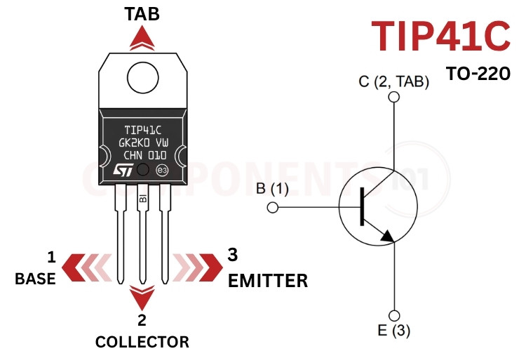
TIP41C Pinout Configuration
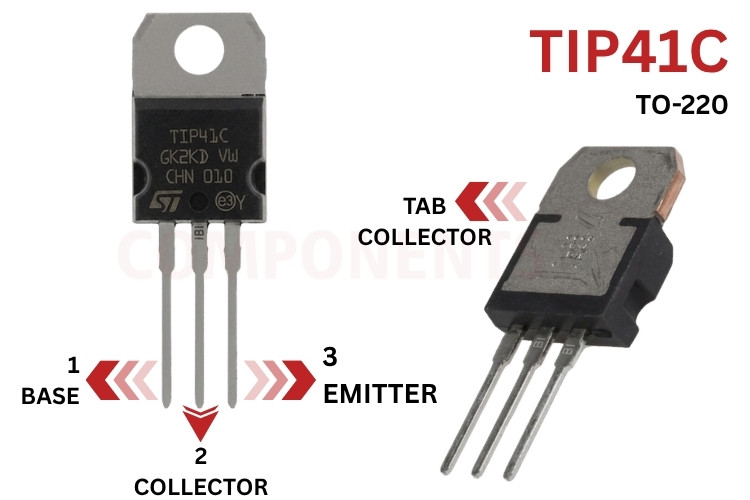
The TIP41C transistor is a 100V, 6A NPN power transistor in a TO-220 package.
| Pin Number | Pin Name | Description |
| 1 | Base (B) | Controls the transistor conduction state. Base current controls the larger collector-to-emitter current flow. |
| 2 | Collector (C) | High-current collector terminal connected to the load. Internally bonded to the metallic heatsink tab. |
| 3 | Emitter (E) | Power return terminal through which total collector and base currents exit to ground or the negative rail. |
| Tab | Collector (C) | Metal mounting tab electrically tied to Pin 2 Collector for heatsink heat dissipation. |
TIP41 Series Voltage Grades: TIP41 vs TIP41A vs TIP41B vs TIP41C
The TIP41 series is manufactured in four distinct collector-emitter breakdown voltage grades. The letter suffix printed on the TO-220 package designates the maximum working voltage:
| Model Variant | Collector-Emitter Voltage (VCEO) | Collector-Base Voltage (VCBO) | Continuous Collector Current (IC) | Typical Application Voltage |
| TIP41 | 40V | 40V | 6A | Low-voltage 12V automotive and battery gadgets. |
| TIP41A | 60V | 60V | 6A | Standard 24V industrial control and relay drivers. |
| TIP41B | 80V | 80V | 6A | 36V to 48V power supplies and medium audio amplifiers. |
| TIP41C | 100V | 100V | 6A | Premium high-voltage tier; universal replacement for all lower tiers |
*Note: Because the TIP41C provides the highest 100V rating while maintaining identical pinout, current capacity, and pricing, electronics designers and repair technicians standardise on TIP41C as a drop-in replacement across all TIP41, TIP41A, and TIP41B circuits.
TIP41C Key Features & Specifications
- Transistor Polarity / Type: NPN Epitaxial-Base Silicon Power Transistor
- Collector-Emitter Voltage (VCEO): 100V (IB = 0)
- Collector-Base Voltage (VCBO): 100V (IE = 0)
- Emitter-Base Voltage (VEBO): 5.0V (IC = 0)
- Continuous Collector Current (IC): 6.0A
- Peak Pulsed Collector Current (ICM): 10.0A
- Continuous Base Current (IB): 2.0A (STMicroelectronics models rated up to 3.0A)
- Total Power Dissipation (PD): 65W at TC = 25°C (2.0W at ambient TA = 25°C without heatsink)
- Collector-Emitter Saturation Voltage (VCE(sat)): 1.5V max at IC = 6.0A, IB = 600 mA
- Base-Emitter On Voltage (VBE(on)): 2.0V max at VCE = 4.0V, IC = 6.0A
- DC Current Gain (hFE): 30 min (at VCE = 4V, IC = 0.3A); 15 to 75 (at VCE = 4V, IC = 3.0A)
- Transition Frequency (fT): 3.0 MHz min at VCE = 10V, IC = 0.5A, f = 1.0 MHz
- Operating Junction Temperature (Tj): -65°C to +150°C
- Thermal Resistance (RthJC): 1.92 °C/W (Junction-to-Case)
- Package Type: TO-220 (TO-220AB / 3-Pin Through-Hole)
*Note: Complete Technical Details can be found in the TIP41C datasheet given at the end of this page.
TIP41C Equivalent & Alternative Components
The best TIP41C equivalent depends on what you need: the same ratings, a complementary PNP, more current, or easier microcontroller drive.
| Equivalent Part | Polarity | Key Ratings | Description & Compatibility Notes |
| TIP42C | PNP | -100V, -6A, 65W, TO-220 | Exact complementary PNP partner for push-pull audio amplifier output stages. |
| BD243C | NPN | 100V, 6A, 65W, TO-220 | European standard direct equivalent with identical pinout and electrical parameters. |
| TIP31C | NPN | 100V, 3A, 40W, TO-220 | Lower-current (3A) sibling; suitable if load current does not exceed 2A. |
| MJE3055T | NPN | 60V, 10A, 75W, TO-220 | Higher current alternative in TO-220 for circuits operating below 60V. |
| 2N3055 | NPN | 60V-100V, 15A, 115W, TO-3 | Heavy-duty metal can power transistors for high-wattage power supplies. |
| TIP122 | NPN | 100V, 5A, Darlington, TO-220 | High-gain Darlington alternative (hFE > 1000) for direct low-current MCU driving. |
What Is the TIP41C Transistor?
The TIP41C is one of the most widely deployed power bipolar transistors in electronic engineering history. Unlike small-signal transistors (such as the BC547 or 2N2222) which are restricted to currents below 800 mA, the TIP41C is engineered to drive medium-power inductive and resistive loads up to 6A continuously when mounted on an appropriate heatsink.
Key design considerations when using the TIP41C include:
1. Base Drive Current Requirements: Because the TIP41C is a standard power BJT (not a Darlington), its DC gain (hFE) decreases at higher collector currents. At IC = 3A, hFE drops to roughly 15 to 30. To fully saturate the transistor and minimize collector-emitter dissipation at 3A load current, the base must receive at least 150 mA to 200 mA of base current (IB ≥ IC / 15).
2. Thermal Dissipation & Heatsinking: In free air without a heatsink, the TO-220 package can only dissipate approximately 2W before its junction temperature exceeds safe limits. When switching or regulating high currents where power dissipation (PD = VCE × IC) exceeds 2W, an aluminum heatsink with thermal paste is mandatory.
3. Collector-Tab Electrical Connection: The metallic mounting tab of the TO-220 package is electrically connected to Pin 2 Collector. When mounting the TIP41C to a shared chassis or grounded heatsink, a mica or silicone insulator pad with an insulating bushing must be installed to prevent shorting the supply rail to ground.
TIP41C Datasheet
The full manufacturer technical documentation, safe operating area (SOA) curves, current gain linearity plots, and thermal resistance ratings are provided in the official STMicroelectronics PDF TIP41C datasheet.
TIP41C Circuit Diagram: DC Motor Driver with Microcontroller PWM
A frequent real-world application of the TIP41C is driving high-current inductive loads (such as 12V or 24V DC motors, heavy solenoids, and high-intensity LED arrays) from the low-voltage PWM output of a microcontroller (Arduino, ESP32, STM32, or 555 timer). The TIP41C circuit diagram below shows the basic low-side switch.
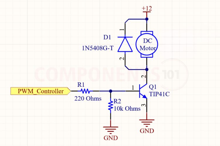
Circuit Operation & Component Selection
1. Base Drive Resistor (RB = 220 Ω, 0.5W):
Microcontroller GPIO pins output 3.3V or 5V logic. When the MCU output goes HIGH (5V), current flows through base resistor RB into the base-emitter junction (VBE ≈ 0.7V to 1.0V). With RB = 220 Ω, the base current is:
IB = (5V - 0.8V) / 220 Ω ≈ 19 mA.
With an hFE of roughly 30 at low to medium loads, 19 mA of base drive allows the TIP41C to reliably switch loads up to 500 mA to 800 mA. For heavier loads (3A to 6A), an intermediate driver transistor (such as a 2N2222A or BC547) or a logic-level buffer should be used to supply the necessary 150 mA to 300 mA base drive current.
2. Base Pull-Down Resistor (RPD = 10 kΩ):
During microcontroller power-up or firmware flashing, GPIO pins default to a high-impedance (floating) state. A 10 kΩ pull-down resistor connected between Pin 1 (Base) and Pin 3 (Emitter/GND) drains stray charge from the base, ensuring the transistor remains firmly OFF and preventing erratic load activation.
3. Flyback Clamping Diode (1N5408 / 1N5822):
When the TIP41C abruptly switches OFF, the collapsing magnetic field in the motor or solenoid generates a high-voltage reverse inductive spike (back-EMF) that can easily exceed the 100V breakdown rating of the transistor. A 3A fast-recovery or Schottky diode (such as a 1N5408 or 1N5822) connected antiparallel across the motor terminals clamps the voltage spike to the positive rail, protecting the collector junction from avalanche damage.
Applications
- Class AB Audio Amplifiers: Power output stages in Hi-Fi stereo amplifiers, guitar practice amplifiers, active subwoofers, and public address (PA) systems (paired with TIP42C).
- Linear DC Power Supplies: Series-pass regulating transistor in benchtop lab power supplies, battery chargers, and low-noise voltage regulators.
- DC Motor Speed Controllers: Pulse-Width Modulated (PWM) motor drivers for robotics, power tools, electric actuators, and cooling fans.
- Solenoid & Relay Drivers: Heavy-duty switching for industrial valves, door locks, automotive relays, and contactor coils.
- LED Strip Dimming: High-power 12V and 24V single-color or RGB LED lighting dimmer circuits.
- Inverter Switching Stages: Low-frequency 12V DC to 230V AC square-wave and modified sine-wave push-pull inverters.
2D Model and Component Dimensions
For hardware designers laying out PCB footprints in EDA tools (KiCad, Altium Designer, Eagle, EasyEDA), the physical dimensions for the standard TO-220 (TO-220AB) package are detailed below:
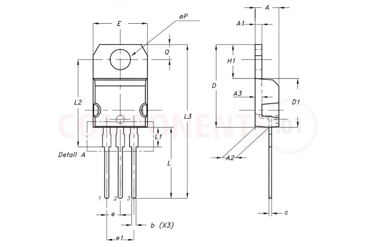
| Parameter Symbol & Description | Minimum (mm) | Typical (mm) | Maximum (mm) |
| A (Package Thickness / Total Depth) | 4.40 | 4.45 | 4.50 |
| A1 (Heatsink Tab Thickness) | 1.22 | - | 1.32 |
| A2 (Base to Seating Plane) | 2.49 | 2.59 | 2.69 |
| A3 (Step Thickness to Tab) | 1.17 | 1.27 | 1.37 |
| b (Lead Width, X3) | 0.78 | - | 0.87 |
| c (Lead Thickness) | 0.49 | - | 0.56 |
| D (Total Body Length / Height) | 15.40 | 15.50 | 15.60 |
| D1 (Lower Molded Body Height) | 9.05 | 9.15 | 9.25 |
| E (Total Body Width) | 10.08 | 10.18 | 10.28 |
| e (Lead Pitch / Pin Spacing) | 2.44 | 2.54 | 2.64 |
| e1 (Total Pin 1 to Pin 3 Spacing) | 4.98 | 5.08 | 5.18 |
| H1 (Heatsink Tab Height) | 6.25 | 6.35 | 6.45 |
| L (Lead Length from Body) | 13.20 | 13.40 | 13.60 |
| L1 (Lead Shoulder Length) | 3.50 | 3.70 | 3.90 |
| L2 (Hole Center to Lead Shoulder) | 16.30 | 16.40 | 16.50 |
| L3 (Overall Package Length with Leads) | 28.70 | 28.90 | 29.10 |
| ØP (Mounting Hole Diameter) | 3.75 | 3.80 | 3.85 |
| Q (Tab Top to Hole Center) | 2.70 | 2.80 | 2.90 |