ATMega328P Microcontroller
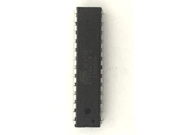
ATMEGA328P is high performance, low power controller from Microchip. ATMEGA328P is an 8-bit microcontroller based on AVR RISC architecture. It is the most popular of all AVR controllers as it is used in ARDUINO boards.
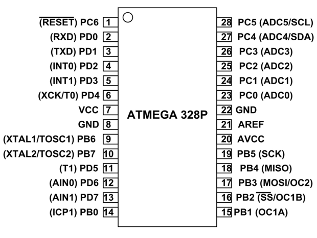
ATMega328 Pinout Configuration
ATMEGA328P is a 28 pin chip as shown in pin diagram above. Many pins of the chip here have more than one function. We will describe functions of each pin in below table.
|
Pin No. |
Pin name |
Description |
Secondary Function |
|
1 |
PC6 (RESET) |
Pin6 of PORTC |
Pin by default is used as RESET pin. PC6 can only be used as I/O pin when RSTDISBL Fuse is programmed. |
|
2 |
PD0 (RXD) |
Pin0 of PORTD |
RXD (Data Input Pin for USART) USART Serial Communication Interface [Can be used for programming] |
|
3 |
PD1 (TXD) |
Pin1 of PORTD |
TXD (Data Output Pin for USART) USART Serial Communication Interface [Can be used for programming]
INT2( External Interrupt 2 Input) |
|
4 |
PD2 (INT0) |
Pin2 of PORTD |
External Interrupt source 0
|
|
5 |
PD3 (INT1/OC2B) |
Pin3 of PORTD |
External Interrupt source1
OC2B(PWM - Timer/Counter2 Output Compare Match B Output) |
|
6 |
PD4 (XCK/T0) |
Pin4 of PORTD |
T0( Timer0 External Counter Input) XCK ( USART External Clock I/O) |
|
7 |
VCC |
Connected to positive voltage |
|
|
8 |
GND |
Connected to ground |
|
|
9 |
PB6 (XTAL1/TOSC1) |
Pin6 of PORTB |
XTAL1 (Chip Clock Oscillator pin 1 or External clock input) TOSC1 (Timer Oscillator pin 1) |
|
10 |
PB7 (XTAL2/TOSC2) |
Pin7 of PORTB |
XTAL2 (Chip Clock Oscillator pin 2) TOSC2 (Timer Oscillator pin 2) |
|
11 |
PD5 (T1/OC0B) |
Pin5 of PORTD |
T1(Timer1 External Counter Input)
OC0B(PWM - Timer/Counter0 Output Compare Match B Output) |
|
12 |
PD6 (AIN0/OC0A) |
Pin6 of PORTD |
AIN0(Analog Comparator Positive I/P)
OC0A(PWM - Timer/Counter0 Output Compare Match A Output) |
|
13 |
PD7 (AIN1) |
Pin7 of PORTD |
AIN1(Analog Comparator Negative I/P)
|
|
14 |
PB0 (ICP1/CLKO) |
Pin0 of PORTB |
ICP1(Timer/Counter1 Input Capture Pin)
CLKO (Divided System Clock. The divided system clock can be output on the PB0 pin) |
|
15 |
PB1 (OC1A) |
Pin1 of PORTB |
OC1A (Timer/Counter1 Output Compare Match A Output) |
|
16 |
PB2 (SS/OC1B) |
Pin2 of PORTB |
SS (SPI Slave Select Input). This pin is low when controller acts as slave. [Serial Peripheral Interface (SPI) for programming]
OC1B (Timer/Counter1 Output Compare Match B Output) |
|
17 |
PB3 (MOSI/OC2A) |
Pin3 of PORTB |
MOSI (Master Output Slave Input). When controller acts as slave, the data is received by this pin. [Serial Peripheral Interface (SPI) for programming] OC2 (Timer/Counter2 Output Compare Match Output) |
|
18 |
PB4 (MISO) |
Pin4 of PORTB |
MISO (Master Input Slave Output). When controller acts as slave, the data is sent to master by this controller through this pin.
[Serial Peripheral Interface (SPI) for programming] |
|
19 |
PB5 (SCK) |
Pin5 of PORTB |
SCK (SPI Bus Serial Clock). This is the clock shared between this controller and other system for accurate data transfer. [Serial Peripheral Interface (SPI) for programming] |
|
20 |
AVCC |
Power for Internal ADC Converter |
|
|
21 |
AREF |
Analog Reference Pin for ADC |
|
|
22 |
GND |
GROUND |
|
|
23 |
PC0 (ADC0) |
Pin0 of PORTC |
ADC0 (ADC Input Channel 0) |
|
24 |
PC1 (ADC1) |
Pin1 of PORTC |
ADC1 (ADC Input Channel 1) |
|
25 |
PC2 (ADC2) |
Pin2 of PORTC |
ADC2 (ADC Input Channel 2) |
|
26 |
PC3 (ADC3) |
Pin3 of PORTC |
ADC3 (ADC Input Channel 3) |
|
27 |
PC4 (ADC4/SDA) |
Pin4 of PORTC |
ADC4 (ADC Input Channel 4) SDA (Two-wire Serial Bus Data Input/output Line) |
|
28 |
PC5 (ADC5/SCL) |
Pin5 of PORTC |
ADC5 (ADC Input Channel 5) SCL (Two-wire Serial Bus Clock Line) |
Features
|
ATMEGA328P – Simplified Features |
|
|
CPU |
8-bit AVR |
|
Number of Pins |
28 |
|
Operating Voltage (V) |
+1.8 V TO +5.5V |
|
Number of programmable I/O lines |
23 |
|
Communication Interface |
Master/Slave SPI Serial Interface(17,18,19 PINS) [Can be used for programming this controller] Programmable Serial USART(2,3 PINS) [Can be used for programming this controller] Two-wire Serial Interface(27,28 PINS)[Can be used to connect peripheral devices like Servos, sensors and memory devices] |
|
JTAG Interface |
Not available |
|
ADC Module |
6channels, 10-bit resolution ADC |
|
Timer Module |
Two 8-bit counters with Separate Prescaler and compare mode, One 16-bit counter with Separate Prescaler,compare mode and capture mode. |
|
Analog Comparators |
1(12,13 PINS) |
|
DAC Module |
Nil |
|
PWM channels |
6 |
|
External Oscillator |
0-4MHz @ 1.8V to 5.5V 0-10MHz @ 2.7V to 5.5V 0-20MHz @ 4.5V to 5.5V |
|
Internal Oscillator |
8MHz Calibrated Internal Oscillator |
|
Program Memory Type |
Flash |
|
Program Memory or Flash memory |
32Kbytes[10000 write/erase cycles] |
|
CPU Speed |
1MIPS for 1MHz |
|
RAM |
2Kbytes Internal SRAM |
|
EEPROM |
1Kbytes EEPROM |
|
Watchdog Timer |
Programmable Watchdog Timer with Separate On-chipOscillator |
|
Program Lock |
Yes |
|
Power Save Modes |
Six Modes[Idle, ADC Noise Reduction, Power-save, Power-down, Standby and Extended Standby] |
|
Operating Temperature |
-40°C to +105°C(+105 being absolute maximum, -40 being absolute minimum) |
Note: Complete technical details can be found in the ATMEGA328P Datasheet linked at the bottom of this page.
ATMEGA328P Replacements
ATMEGA328P Alternatives
ATMEGA16, ATMEGA32, ATMEGA8535
Where to Use ATMEGA328P
Although we have many controllers ATMEGA328P is most popular of all because of its features and cost. ARDUINO boards are also developed on this controller because of its features.
- With program memory of 32 Kbytes ATMEGA328P applications are many.
- With various POWER SAVING modes it can work on MOBILE EMBEDDED SYSTEMS.
- With Watchdog timer to reset under error it can be used on systems with minimal human interference.
- With advanced RISC architecture, the controller executes programs quickly.
- Also with in chip temperature sensor the controller can be used at extreme temperatures.
These all features add together promoting ATMEGA328P further.
How to Use ATMEGA328P
ATMEGA328 is used similar to any other controller. All there to do is programming. Controller simply executes the program provided by us at any instant. Without programming controller simply stays put without doing anything.
As said, first we need to program the controller and that is done by writing the appropriate program file in the ATMEGA328P FLASH memory. After dumping this program code, the controller executes this code and provides appropriate response.
Entire process of using an ATMEGA328P goes like this:
- List the functions to be executed by controller.
- Write the functions in programming language in IDE programs.
You can download the IDE program for free in company websites. IDE program for AVR controllers is ‘ATMEL STUDIO’. Link for ATMEL STUDIO is given below.
(Usually Atmel Studio 6.0 for Windows7 [http://atmel-studio.software.informer.com/6.0/],
Atmel Studio 7 for Windows10 [https://www.microchip.com/avr-support/atmel-studio-7])
- ATMEGA328P programming can also be done in ARDUINO IDE.
- After writing the program, compile it to eliminate errors.
- Make the IDE generate HEX file for the written program after compiling.
- This HEX file contains the machine code which should be written in controller flash memory.
- Choose the programming device (usually SPI programmer made for AVR controllers) which establishes communication between PC and ATMEGA328P. You can also program ATMEGA328P using ARDUINO UNO board.
- Run the programmer software and choose the appropriate hex file.
- Burn the HEX file of written program in ATMEGA328P flash memory using this program.
- Disconnect the programmer, connect the appropriate peripherals for the controller and get the system started.
How to Use ATMega328P using Arduino
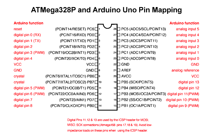
Since ATmega328P is used in Arduino Uno and Arduino nano boards, you can directly replace the arduino board with ATmega328 chip. For that first you need to install the Arduino bootloader into the chip (Or you can also buy a chip with bootloader – ATMega328P-PU). This IC with bootloader can be placed on Arduino Uno board and burn the program into it. Once Arduino program is burnt into the IC, it can be removed and used in place of Arduino board, along with a Crystal oscillator and other components as required for the project. Below is the pin mapping between Arduino Uno and ATmega328P chip.
Applications
There are hundreds of applications for ATMEGA328P:
- Used in ARDUINO UNO, ARDUINO NANO and ARDUINO MICRO boards.
- Industrial control systems.
- SMPS and Power Regulation systems.
- Digital data processing.
- Analog signal measuring and manipulations.
- Embedded systems like coffee machine, vending machine.
- Motor control systems.
- Display units.
- Peripheral Interface system.
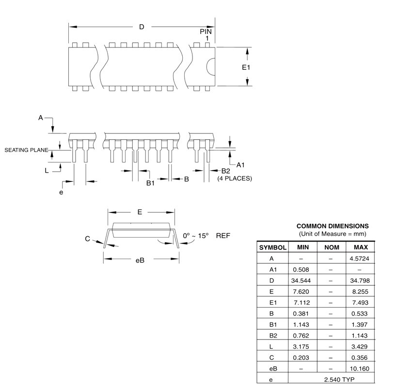
2D Model and Dimensions
All measurements are in millimeters.