LM741 Op-amp IC

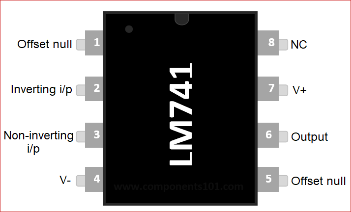
LM741 Pin Configuration
|
Pin Number |
Pin Name |
Description |
|
1 , 5 |
OFFSET NULL |
Pin used for remove the offset voltage and balance input voltage. |
|
2 |
INPUT- |
Inverting signal Input |
|
3 |
INPUT+ |
Non-Inverting signal Input |
|
4 |
V- |
Ground or Negative Supply Voltage |
|
6 |
OUTPUT |
Output of op amp |
|
7 |
V+ |
Positive Supply Voltage |
|
8 |
NC |
Not connected |
LM741 Op-Amp IC Features and Specifications
- LM741 has only one op-amp inside, there are some op-amp IC’s having more than one op-amp like LM358, LM148, LM248, LM348
- Provided with short circuit and overload protection.
- Low power consumption.
- Large common mode rejection ratio (CMRR) and differential voltage ranges.
- No external frequency compensation is required.
- Prevent from latch-up when common-mode range is exceeded.
- Minimum, normal and maximum Power Consumption for this IC is ±10v, ±15v and ±22v respectively.
- Operating temperature should be -50 to 125 ˚C.
- Supply current – 1.7 to 2.8mA.
- Soldering pin temperature – PDIP package - 260 ˚C (for 10 seconds – prescribed)
- TO-99 and CDIP - 300 ˚C (for 10 seconds – prescribed)
- Available packages: TO-99, CDIP & PDIP
LM741 Equivalent Op-Amp ICs
LM741A, LM741C, LM709C, LM201, MC1439, and LM748
Brief Description
An LM741 operational amplifier is a DC-coupled high gain electronic voltage amplifier. It has only one op-amp inside. An operational amplifier IC is used as a comparator which compares the two signal, the inverting and non-inverting signal. The main function of this IC is to do mathematical operation in various circuits. Op-amps have large gain and usually used as Voltage Amplifier. The LM741 can operate with a single or dual power supply voltage.
OUTPUT Voltage = Gain * Input Voltage
An op-amp can be used in two ways:
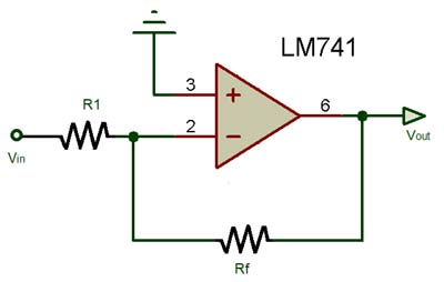
1. Inverting Op-amp
When input source is connected to inverting terminal PIN 2 and feedback with the output PIN 6 then the op-amp is in inverting condition. Like if PIN 2 is having +ve polarity then we will get –ve polarity of output from PIN 6.
GAIN = Rf/R1
2. Non-inverting Op-amp
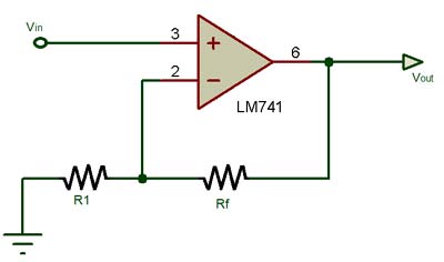
When input source is connected to non-inverting terminal PIN 3 and PIN 2 is feedback with the output PIN 6 then the op-amp is in non-inverting condition. Like if PIN 3 is having +ve polarity then we will get +ve polarity of output from PIN 6.
GAIN = 1+ (Rf/R1)
Working Concept
When voltage at non-inverting input (+) is higher than the voltage at inverting input (-), then the output of comparator is HIGH. And if the voltage of inverting input (-) is Higher than non-inverting end (+), then output is LOW. The output of the operational amplifier is the product of the gain and the input voltage.
LM741 Applications
- Comparators
- DC Amplifiers
- Integrator or Differentiators
- Summing Amplifiers
- Multi-vibrators
- Active Filters
- General feedback applications
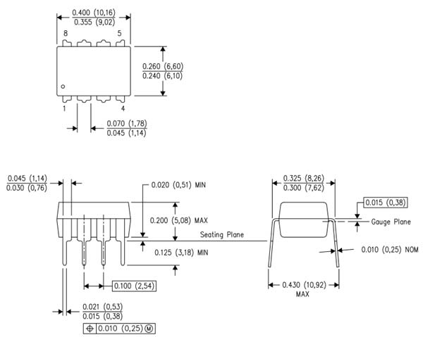
2D-Model
In Op-amp IC 741, PIN2 is an inverting input terminal and PIN3 is non-inverting input terminal. The output pin of this IC is PIN6.