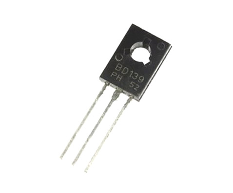
BD139 Transistor
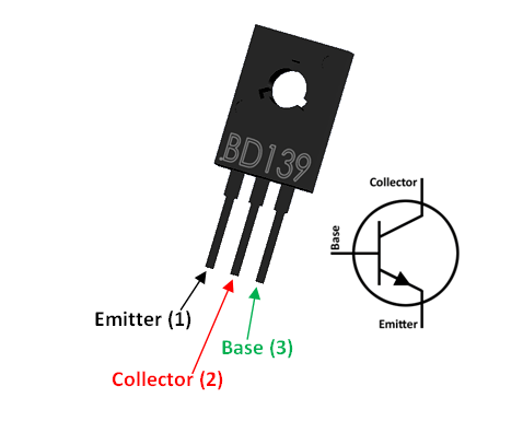
BD139 Pinout Configuration
|
Pin Number |
Pin Name |
Description |
|
1 |
Emitter |
Current Drains out through emitter, normally connected to ground |
|
2 |
Collector |
Current flows in through collector, normally connected to load |
|
3 |
Base |
Controls the biasing of transistor, Used to turn ON or OFF the transistor. |
Features
- Plastic casing NPN Transistor
- Continuous Collector current (IC) is 1.5A
- Collector-Emitter voltage (VCE) is 80 V
- Collector-Base voltage (VCB) is 80V
- Base Current (Ib) is 0.5A
- Emitter Base Breakdown Voltage (VBE) is 5V
- DC current gain (hfe) is 40 to 160
- Available in To-225 package
Note: Complete Technical Details can be found at the BD139 transistor datasheet provided at the bottom of this page.
BD139 Equivalent NPN Transistors
BD136, BD138, BD140
Alternative to BD139 Transistor
D882
Other NPN Transistors
TIP31C, SL100, S8050, BC547, 2N2222, 2N4401
BD139 Transistor Overview
BD139 is a NPN transistor hence the collector and emitter will be left open (Reverse biased) when the base pin is held at ground and will be closed (Forward biased) when a signal is provided to base pin
BD139 has a gain value of 40 to 160, this value determines the amplification capacity of the transistor. The maximum amount of current that could flow through the Collector pin is 1.5A, hence we cannot connect loads that consume more than 1.5A using this transistor. To bias a transistor we have to supply current to base pin, this current (IB) should be limited to 1/10th of the collector current and voltage across the base emitter pin should be 5V maximum.
When this transistor is fully biased then it can allow a maximum of 1.5A to flow across the collector and emitter. This stage is called Saturation Region and the typical voltage allowed across the Collector-Emitter (VCE) or Base-Emitter (VBE) could be 80V. When base current is removed the transistor becomes fully off, this stage is called as the Cut-off Region.
The BD139 was originally manufactured by Phillips rated at 160MHz for specific audio applications, later they were cloned by other manufacturers like Samsung, ST etc.
Where to use BD136 Transistor
Being a Medium Power NPN Transistor with a collector current of 1.5A this transistor can be used to control (On/Off) bigger loads that consume less than 1.5A. It also has a very less saturation voltage (Base Emitter Voltage VBE) of only 5V, this makes it easy to use this IC in digital electronics which has an operating voltage of 5V.
Another peculiar fact about this transistor is that it comes in plastic package, while most medium power transistor are available only in metal can package. This reduces the cost of the Transistor and also since the package is not conductive it will not be affected by other noise in the circuit. Due to this feature this transistor is widely used in amplifier applications.
So if you are looking for a medium power NPN transistor in Plastic package then this Transistor might be the right choice for you.
Applications
- RF Amplifiers
- Switching circuits
- Amplification circuits
- Audio amplifiers
- Load driver circuits
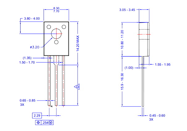
Dimensions (TO-225)


Missing Information | Base Current
I came to this website to know about the base current of the BD139 transistor, but it's very disappointing to see that the author did not even mention the base current.