AHV85003 and AHV85043 isolated SiC gate driver chipsets are optimized for driving discrete SiC FETs
Buck Converter: Basics, Working, Design and Operation
Many a times in the electronics world we find the need to reduce one DC voltage to a lower one. For example we may need to power a 3.3V microcontroller from a 12V supply rail. The solution is simple, we just add a 3.3V linear regulator IC like LD1117 with the 12V rail and it regulates the voltage down to 3.3V. We have already learnt the working of Voltage regulators in our previous article.
Now, suppose we have to power an LED strip from the same 3.3V rail. LEDs easily consume around 20mA each, so a long strip would easily eat up an amp or so. If we calculate the power dissipated by the regulator:
P = (Vin – Vout) * Iout
The power dissipated comes out to be around 8.7 Watts! Now this is a LOT of power for a little linear regulator to dissipate. If we calculate the efficiency, which is just output power divided by the input power, it comes out to be a pathetic 38%!. Normally Linear voltage regulators has very low efficiency compared with switching regulators.
Now we feel the pressing need to find something that can step DC voltages down and do it efficiently!
Introduction to Buck Converters
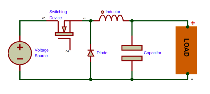
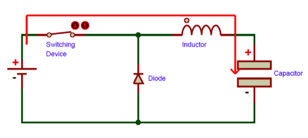
Luckily such a device already exists, and it’s called a buck converter or step down voltage regulators. It’s a type of DC-DC converter, so it accomplishes the task using a few transistor switches and an inductor. A typical buck converter circuit is shown in the above image.
It’s quite similar to a boost converter, but the placement of the inductor and transistor are switched. The switch shown in the above circuit will normally be a power electronics switch like MOSFET, IGBT or BJT. The switch will be switched (turned on and off) by using a PWM signal.
The working of Buck converter is slightly similar to that of PWM ‘dimming’. We’ve all heard of lights being dimmed by a PWM signal. A small duty cycle means that the average voltage seen by the load is small and when the duty cycle is high the average voltage is high too.
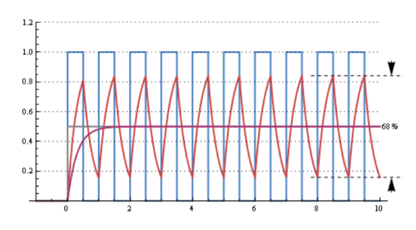
But average voltage is not what we need – a raw PWN signal oscillates between high voltage level and ground, something no delicate load (like the microcontroller) would like. Of course, connecting an RC filter to a square wave source renders the output clean. The voltage level of the filter depends on the duty cycle of the PWM signal – the higher the duty cycle the higher the output voltage.
So now we have a clean output voltage. The below graph shows the raw PWM signal in blue color and the filtered outputs in red and violet color.
We could now simply use this as a buck converter, but there’s one major drawback –the resistor in the RC filter limits the current and wastes energy in the form of heat, which is no better than the linear voltage regulator example.
To fix this problem, we turn to another type of voltage filter, the LC filter, which does the same job as the RC filter but replaces the R with an L, in other words the resistor with an inductor. The inductor resists changes in current and the capacitor resists changes in voltage, which results in the output being smooth DC.
And now we have a converter that is capable of stepping down DC voltages and doing it efficiently!
Working of a Buck Converter
The working of a buck converter can be broken down into a few steps.
STEP – 1:
The switch turns on and lets current flow to the output capacitor, charging it up. Since the voltage across the capacitor cannot rise instantly, and since the inductor limits the charging current, the voltage across the cap during the switching cycle is not the full voltage of the power source.
STEP – 2:
The switch now turns off. Since the current in an inductor cannot change suddenly, the inductor creates a voltage across it. This voltage is allowed to charge the capacitor and power the load through the diode when the switch is turned off, maintaining current output current throughout the switching cycle.
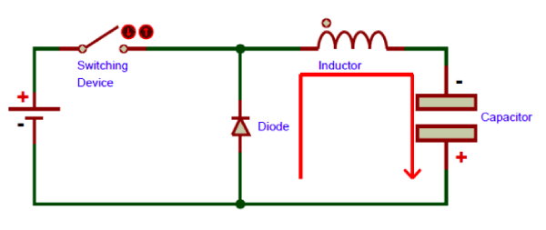
These two steps keep repeating many thousands of times a second, resulting in continuous output.
Designing a Buck Converter
STEP – 1
Determine the input voltage and the output voltage and current.
The duty cycle of the converter is given by:
DC = Vout/Vin
STEP – 2
Determine the output power, that is, the product of the output voltage and current. This is also the input power, by the law of conservation of energy (though not exactly so – nothing is a hundred percent efficient!).
STEP - 3
Now divide the output power by the selected switching frequency in order to get the power transferred per pulse.
Since it is easier to talk about inductors in terms of energy, we can assume now that the output power is simply the output energy per second. So if the output of our converter is 30 Watts, then we can say that the output energy is thirty Joules every second.
STEP - 4
Now that we have the energy per pulse, we can calculate the inductance using the input current and the energy:
L = 2E/I2
Where E is the energy transferred per pulse and I is the square of the input current.
Using the values of the inductance, frequency and duty cycle, we can now get to work building a simple boost converter.
Choice of Parts
MOSFET
Since the switch is on the high side, using an N channel MOSFET or an NPN bipolar wouldn’t work, unless we have a bootstrapped gate driver. Though this is possible, it is quite complicated.
Using a P channel device in these circumstances would be recommended, they greatly simplify driving requirements, but remember that they turn on when the gate is low, so an inverted signal would be necessary. One can use the IRF5210, it has a decent on resistance of 60mΩ and a VDS of -100V,which should be plenty for most applications. However, there are many better devices available, the choice is entirely up to the designer based on the specific application.
Remember to use a gate driver to reduce switching losses!
DIODE
Since this diode does not have to handle very high voltages, rather high currents, it would be a good design choice to use a Schottky diode with a low forward voltage drop to keep things efficient.
CAPACITOR
The capacitor value depends on the output voltage ripple and can be calculated using the capacitor equation, but generally a value between 100uF to 680uF for low current applications should suffice.
Conclusion
Remember, the design process described here should not be treated as an expert rant, rather these are very simple equations to get your first buck converter up and running.
Again, regulation is a topic that has not been covered here. If you want to make a regulated buck converter, it is recommended to use a dedicated buck controller IC like LM2596 designed specifically for that purpose.


