IRFB4110 N-Channel Power MOSFET Pinout, Specifications, Equivalent & Datasheet
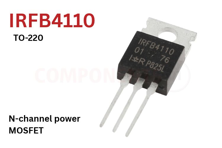
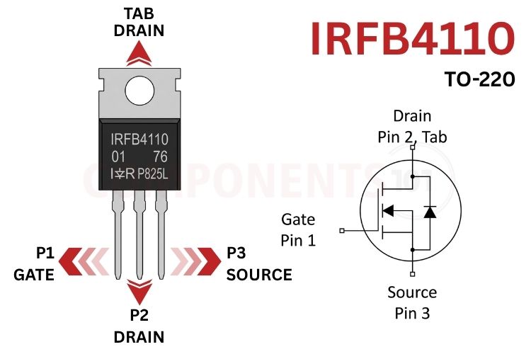
IRFB4110 Pinout Configuration
The IRFB4110 follows the standard JEDEC TO-220AB 3-pin configuration:
| Pin Number | Pin Name | Description |
| 1 | Gate (G) | Voltage control terminal. Applying +10V to +12V relative to Source drives the channel into deep saturation with minimum RDS(on) |
| 2 | Drain (D) | High-current power terminal connected to the load or motor phase and internally bonded to the metallic TO-220 mounting heatsink tab. |
| 3 | Source (S) | Power terminal connected to system ground (common return) or a low-side current sensing shunt resistor. |
| Tab | Drain (D) | Metallic mounting heatsink tab electrically connected to Pin 2 Drain for maximum thermal transfer to an external heatsink. |
*Note: Because the metallic heatsink tab is bonded to Pin 2 Drain, mounting the IRFB4110 onto a shared grounded chassis or common metal heatsink requires electrical insulation (mica or sil-pad with an insulating shoulder washer) to avoid shorting the switched drain node to ground.
IRFB4110 Key Features & Specifications
- Transistor Polarity / Type: N-Channel Enhancement-Mode HEXFET Power MOSFET
- Drain-to-Source Breakdown Voltage (V(BR)DSS): 100V (at VGS = 0V, ID = 250 µA)
- Continuous Drain Current (ID) at TC = 25°C: 180A (silicon limited); 120A (package lead limited)
- Pulsed Drain Current (IDM): 670A (pulse width limited by maximum junction temperature)
- Maximum Power Dissipation (PD): 370W at TC = 25°C (linear derating factor 2.5 W/°C above 25°C)
- Static Drain-to-Source On-Resistance (RDS(on)): 3.7 mΩ typ, 4.5 mΩ max at VGS = 10V, ID = 75A
- Gate Threshold Voltage (VGS(th)): 2.0V min to 4.0V max at VDS = VGS, ID = 250 µA
- Forward Transconductance (gfs): 160 S min at VDS = 50V, ID = 75A
- Total Gate Charge (Qg): 150 nC typ, 230 nC max at VGS = 10V, ID = 75A, VDS = 50V
- Gate-to-Source Charge (Qgs): 39 nC typ; Gate-to-Drain Charge (Qgd): 50 nC typ
- Input Capacitance (Ciss): 9620 pF typ at VDS = 50V, VGS = 0V, f = 1.0 MHz
- Output Capacitance (Coss): 680 pF typ; Reverse Transfer Capacitance (Crss): 250 pF typ
- Turn-On Delay Time (td(on)): 25 ns typ; Rise Time (tr): 67 ns typ (VDD = 65V, ID = 75A, RG = 2.6 Ω)
- Turn-Off Delay Time (td(off)): 78 ns typ; Fall Time (tf): 58 ns typ
- Avalanche Current (IAR): 75A max
- Peak Diode Recovery (dv/dt): 15 V/ns max (ISD ≤ 75A, di/dt ≤ 600 A/µs, VDD ≤ 100V)
- Body Diode Forward Voltage (VSD): 1.3V max at ISD = 75A, VGS = 0V
- Package Type: TO-220AB (Through-Hole 3-Lead Power Package, Infineon PG-TO220-3-U05)
*Note: Complete Technical Details can be found in the IRFB4110 datasheet given at the end of this page.
IRFB4110 Equivalent & Alternative Components
| Equivalent Part | Polarity | Key Ratings | Description & Compatibility Notes |
| IRFB4110PBF | N-Channel | 100V, 180A (120A pkg), 4.5 mΩ, TO-220AB | Direct lead-free, RoHS-compliant exact drop-in replacement by Infineon / IR. |
| IRFB3077 | N-Channel | 75V, 210A (120A pkg), 3.3 mΩ, TO-220AB | Higher current and lower RDS(on) sibling for 36V-48V battery systems where 75V breakdown margin is sufficient. |
| IRFB4310 | N-Channel | 100V, 140A (120A pkg), 6.0 mΩ, TO-220AB | Cost-effective 100V sibling with slightly higher on-resistance; ideal for moderate 40A-60A motor stages. |
| IRFB4115 | N-Channel | 150V, 104A, 11 mΩ, TO-220AB | Higher voltage 150V sibling designed for 72V-96V battery systems requiring higher inductive voltage headroom. |
| STP150N10F7 | N-Channel | 100V, 110A, 6.0 mΩ, TO-220 | STMicroelectronics 100V DeepGATE power MOSFET alternative. |
| FDP047N10 | N-Channel | 100V, 164A, 4.7 mΩ, TO-220 | Fairchild / onsemi PowerTrench 100V N-channel MOSFET with comparable sub-5 mΩ resistance. |
| IPP041N12N3 G | N-Channel | 120V, 120A, 4.1 mΩ, TO-220 | Infineon OptiMOS 3 upgrade offering higher voltage (120V) and ultra-low conduction losses. |
Brief Description of IRFB4110
The IRFB4110 MOSFET is the benchmark discrete power MOSFET for high-current, medium-voltage power electronic circuits. Built on Infineon's planar stripe cell process, it establishes an extraordinary balance between ultra-low conduction resistance (4.5 mΩ max) and superior ruggedness under severe switching transients.
Key design considerations when integrating the IRFB4110 include:
- Silicon vs. Package Current Limit: Although the IRFB4110 die is rated for 180 A, the TO-220AB package limits continuous terminal current to around 120 A. Above 60-80 A, reinforced PCB copper and careful thermal design are essential.
- Gate Drive & High Gate Charge: With 9620 pF Ciss and 150 nC Qg, direct MCU GPIO driving causes slow switching and excessive heating. For 10-50 kHz PWM, use a dedicated 2-6 A peak gate driver with a ~12 V gate supply.
- Thermal Dissipation: With RθJC = 0.40°C/W and 4.5 mΩ RDS(on), conduction loss at 50 A is approximately 11.25 W. A suitable heatsink and, at higher power, forced-air cooling are required.
- Inductive Kickback: The 990 mJ single-pulse avalanche rating protects against short-duration voltage spikes generated by inductive loads during switching.
IRFB4110 Datasheet
The complete manufacturer electrical characteristics, safe operating area (SOA) curves, thermal impedance charts, and avalanche energy test circuits are available in the official Infineon PDF IRFB4110 Datasheet.
How to Use the IRFB4110 in a Circuit
The schematic below shows a high-power 48V to 72V DC motor PWM speed controller that uses the IRFB4110 as a low-side power switch, driven by a TC4420 6A high-speed, non-inverting MOSFET gate driver IC.
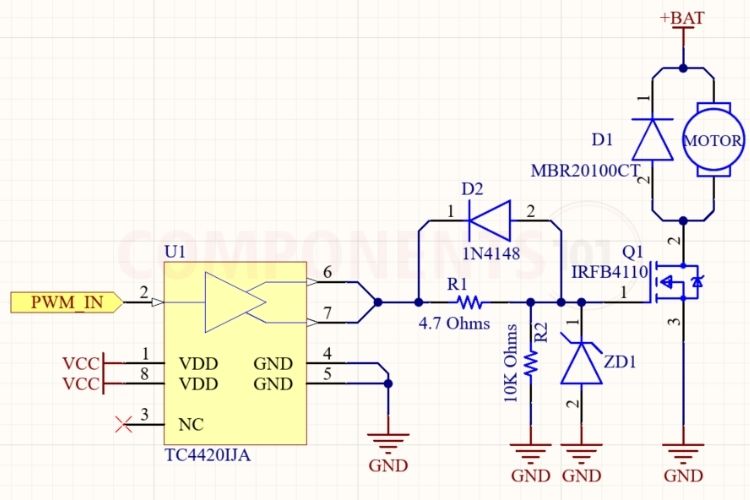
1. Dedicated Gate Driver IC (TC4420):
Because an Arduino, ESP32, or STM32 microcontroller pin cannot rapidly charge the 9620 pF input capacitance of the IRFB4110, a TC4420 non-inverting driver IC is deployed. Powered from an auxiliary +12V DC rail, the TC4420 translates 3.3V/5V logic PWM signals into sharp 12V gate pulses with rise and fall times under 25 ns, driving the MOSFET gate with up to 6A of peak charging current.
2. Asymmetric Gate Resistor Network:
- Turn-On: The TC4420 charges the gate through resistor R1 (4.7 Ω), dampening parasitic LC ringing between the gate lead inductance and input capacitance, preventing destructive gate voltage spikes.
- Fast Turn-Off: High-speed switching diode D2 (1N4148) connects anti-parallel across R1. During turn-off, D2 bypasses the gate resistor, allowing the driver to sink gate discharge current directly and rapidly pull the gate to ground, preventing Miller capacitance-induced shoot-through.
3. Gate Protection Clamp (ZD1 = 15V Zener Diode & R2 = 10 kΩ):
- Zener Clamp ZD1 (1N4744A, 15V): Connected directly between Gate and Source, this clamp ensures that transient voltage spikes coupled through drain-to-gate Miller capacitance (Crss = 250 pF) cannot exceed the absolute maximum ±20V VGS rating of the MOSFET.
- Pull-Down Resistor R2 (10 kΩ): Holds the Gate firmly at 0V during microcontroller power-up, reboot, or firmware flashing, preventing accidental motor activation while GPIO pins float in high-impedance mode.
Applications
- Electric Vehicle & E-Bike Controllers: Primary low-side switching MOSFET in 48V, 60V, and 72V 6-FET, 12-FET, and 18-FET brushless DC (BLDC) motor speed controllers (Infineon Xiechang architecture).
- Pure Sine Wave DC-AC Power Inverters: High-current H-bridge switching stages in 48V off-grid solar inverters generating 120V / 230V AC mains power.
- High-Current Brushed DC Motor Drivers: PWM speed control for electric winches, trolling motors, robotics actuators, and heavy golf carts.
- Solar Charge Controllers (MPPT / PWM): Synchronous buck converter switching stages and high-side battery disconnect switches in 48V solar systems.
- High-Power Solid-State Relays (SSR): Contact-free, spark-free DC load switches replacing mechanical contactors in telecommunications and server power distribution units.
- Synchronous Rectification & DC-DC Converters: Secondary-side high-efficiency synchronous rectifiers in high-power telecom power supplies.
2D Model and Component Dimensions
For PCB layout engineers and CAD designers drafting footprint libraries in KiCad, Altium Designer, Eagle, or EasyEDA, the mechanical dimensions for the TO-220AB (Infineon Outline PG-TO220-3-U05) package are detailed below:
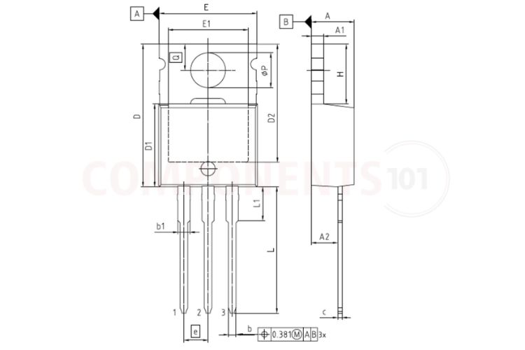
| Parameter Symbol & Description | Minimum (mm) | Typical (mm) | Maximum (mm) |
| A (Total Package Thickness / Depth) | 3.56 | - | 4.83 |
| A1 (Mounting Tab Thickness) | 1.14 | - | 1.40 |
| A2 (Lead Offset / Base to Seating Plane) | 2.03 | - | 2.92 |
| b (Lead Width, X3) | 0.38 | - | 1.01 |
| b1 (Lead Shoulder Width, X3) | 1.14 | - | 1.78 |
| c (Lead Thickness) | 0.36 | - | 0.61 |
| D (Total Body Length / Height) | 14.22 | - | 16.51 |
| D1 (Molded Plastic Body Height) | 8.38 | - | 9.20 |
| D2 (Tab Notch Reference Height) | 11.68 | - | 12.88 |
| E (Total Molded Body Width) | 9.65 | - | 10.67 |
| E1 (Mounting Tab Width) | 6.86 | - | 8.89 |
| e (Lead Pitch / Pin Spacing) | - | 2.54 BSC | - |
| H (Upper Exposed Heatsink Tab Height) | 5.84 | - | 6.86 |
| L (Lead Length Below Seating Plane) | 12.70 | - | 14.73 |
| L1 (Lead Shoulder Length) | 3.56 | - | 4.06 |
| ØP (Mounting Hole Diameter) | 3.54 | - | 4.08 |
| Q (Tab Top to Mounting Hole Center) | 2.54 | - | 3.42 |