TPA3116D2 15-W, 30-W, 50-W Filter-Free Class-D Stereo Amplifier with AM Avoidance
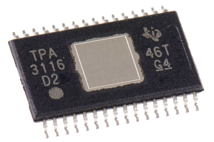
The TPA3116D2 is a Class-D audio amplifier IC from Texas Instruments, designed for multi-function, high power, high fidelity, and compact audio systems. The new amplifier IC was designed with low residual noise, a low distortion ratio, a flat frequency response achieved through feedback technology, and low EMI levels.
The TPA series of ICs can drive up to 100W load with 2Ω impedance in mono configuration, and in order to get the stereo sound, you need to configure and design 2 IC’s. The most interesting feature about this IC is that it can drive 2X15Ω speakers without a heatsink on a dual-layer PCB. This IC features a multifunction PLL IC that can be employed to reduce AM interference. The TPA3116D2 devices are fully protected against faults with short-circuit protection and thermal protection as well as overvoltage, undervoltage, and DC protection. Faults are reported back to the processor to prevent devices from being damaged during overload conditions.
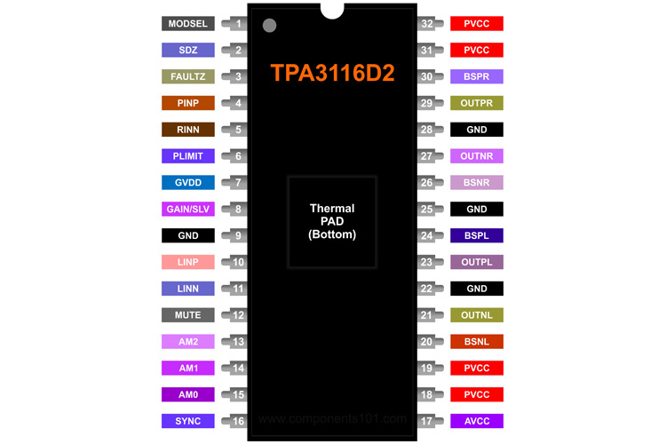
TPA3116D2 Pinout Configuration
|
Pin No. |
Pin Name |
Pin Description |
|
1 |
MODSEL |
Mode selection logic input (LOW = BD mode, HIGH = 1 SPW mode). TTL logic levels with compliance to AVCC. |
|
2 |
SDZ |
Shutdown logic input for audio amp (LOW = outputs Hi-Z, HIGH = outputs enabled). TTL logic levels with compliance to AVCC. |
|
3 |
FAULTZ |
General fault reporting including Over-temp, DC Detect. Open drain. FAULTZ = High, normal operation, FAULTZ = Low, fault condition |
|
4 |
RINP |
Positive audio input for right channel. Biased at 3 V. |
|
5 |
RINN |
Negative audio input for right channel. Biased at 3 V. |
|
6 |
PLIMIT |
Power limit level adjust. Connect a resistor divider from GVDD to GND to set power limit. Connect directly to GVDD for no power limit |
|
7 |
GVDD |
Internally generated gate voltage supply. Not to be used as a supply or connected to any component other than a 1 µF X7R ceramic decoupling capacitor and the PLIMIT and GAIN/SLV resistor dividers |
|
8 |
GAIN/SLV |
Selects Gain and selects between Master and Slave mode depending on pin voltage divider. |
|
9 |
GND |
Ground |
|
10 |
LINP |
Positive audio input for left channel. Biased at 3 V. Connect to GND for PBTL mode |
|
11 |
LINN |
Negative audio input for left channel. Biased at 3 V. Connect to GND for PBTL mode |
|
12 |
MUTE |
Mute signal for fast disable/enable of outputs (HIGH = outputs Hi-Z, LOW = outputs enabled). TTL logic levels with compliance to AVCC. |
|
13 |
AM2 |
AM Avoidance Frequency Selection |
|
14 |
AM1 |
AM Avoidance Frequency Selection |
|
15 |
AM0 |
AM Avoidance Frequency Selection |
|
16 |
SYNC |
Clock input/output for synchronizing multiple class-D devices. Direction determined by GAIN/SLV terminal. |
|
17 |
AVCC |
Analog Supply |
|
18 |
PVCC |
Power supply |
|
19 |
PVCC |
Power supply |
|
20 |
BSNL |
Boot strap for negative left channel output, connect to 220 nF X5R, or better ceramic cap to OUTNL |
|
21 |
OUTNL |
Negative left channel output |
|
22 |
GND |
Ground |
|
23 |
OUTPL |
Positive left channel output |
|
24 |
BSPL |
Boot strap for positive left channel output, connect to 220 nF X5R, or better ceramic cap to OUTPL |
|
25 |
GND |
Ground |
|
26 |
BSNR |
Boot strap for negative right channel output, connect to 220 nF X5R, or better ceramic cap to OUTNR |
|
27 |
OUTNR |
Negative right channel output |
|
28 |
GND |
Ground |
|
29 |
OUTPR |
Positive right channel output |
|
30 |
BSPR |
Boot strap for positive right channel output, connect to 220 nF X5R or better ceramic cap to OUTPR |
|
31 |
PVCC |
Power supply |
|
32 |
PVCC |
Power supply |
|
33 |
PowerPAD |
Connect to GND for best system performance. If not connected to GND, leave floating. |
Features and Specifications
- Supports Multiple Output Configurations
- 2 × 50 W Into a 4-Ω BTL Load at 21 V (TPA3116D2)
- 2 × 30 W Into a 8-Ω BTL Load at 24 V (TPA3118D2)
- 2 × 15 W Into a 8-Ω BTL Load at 15 V (TPA3130D2)
- Wide Voltage Range: 4.5 V to 26 V
- Efficient Class-D Operation
- >90% Power Efficiency Combined with Low Idle Loss Greatly Reduces Heat Sink Size
- Advanced Modulation Schemes
- Multiple Switching Frequencies
- AM Avoidance
- Master and Slave Synchronization
- Up to 1.2-MHz Switching Frequency
- Feedback Power-Stage Architecture with High PSRR Reduces PSU Requirements
- Programmable Power Limit
- Differential and Single-Ended Inputs
- Stereo and Mono Mode with Single-Filter Mono Configuration
- Single Power Supply Reduces Component Count
- Integrated Self-Protection Circuits Including Overvoltage, Undervoltage, Overtemperature, DC Detect, and Short Circuit with Error Reporting
- Thermally Enhanced Packages
- DAD (32-Pin HTSSOP Pad Up)
- DAP (32-Pin HTSSOP Pad Down)
- 40°C to 85°C Ambient Temperature Range
Note: More technical information can be found in the TPA3116D2 Datasheet, linked at the bottom of this page.
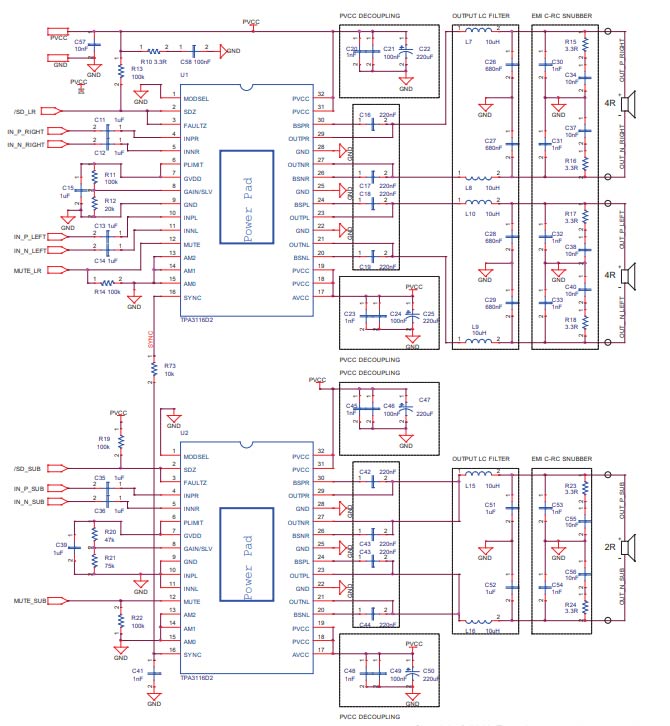
TPA3116D2 CC Typical Application Schematic
The typical application circuit for the TPA3116D2 IC is shown below. For more information please refer to the datasheet linked at the bottom of the webpage.
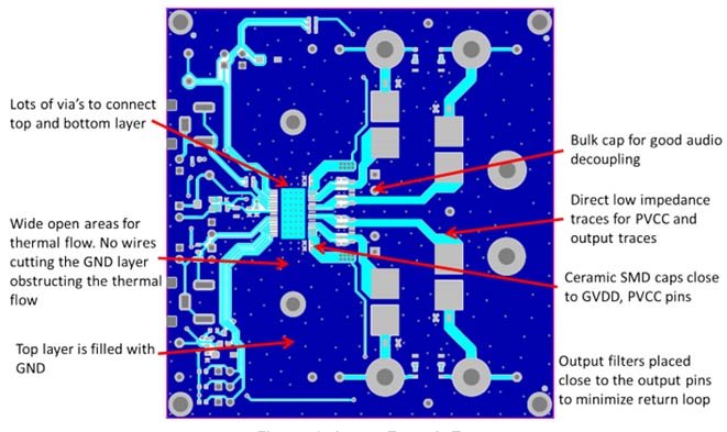
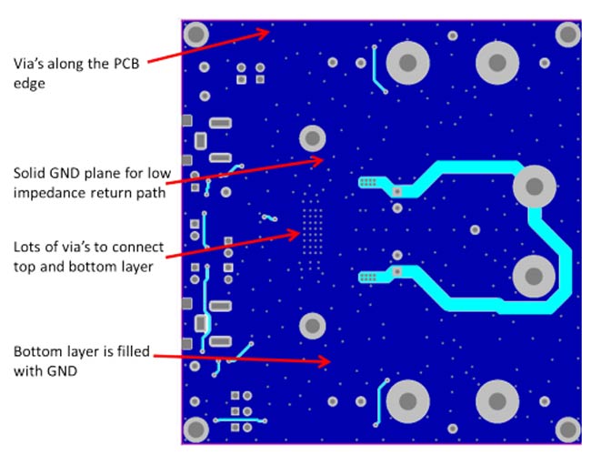
TPA3116D2 CC Typical PCB Layout
The typical PCB layout/ guideline for the TPA3116D2 IC is shown below and for more information please refer to the datasheet linked at the bottom of the webpage.
Top Layer:
Bottom Layer:
Applications
- Mini-Micro Component, Speaker Bar, Docks
- After-Market Automotive
- CRT TV
- Consumer Audio Applications
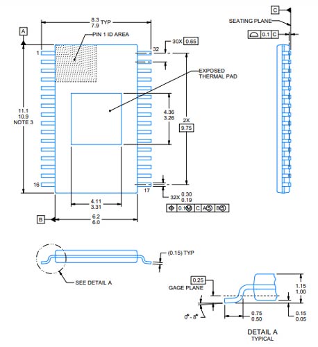
2D Model and Dimensions
If you are designing a PCB or Perf board with this component then the following picture from the Datasheet will be useful to know its package type and dimensions.