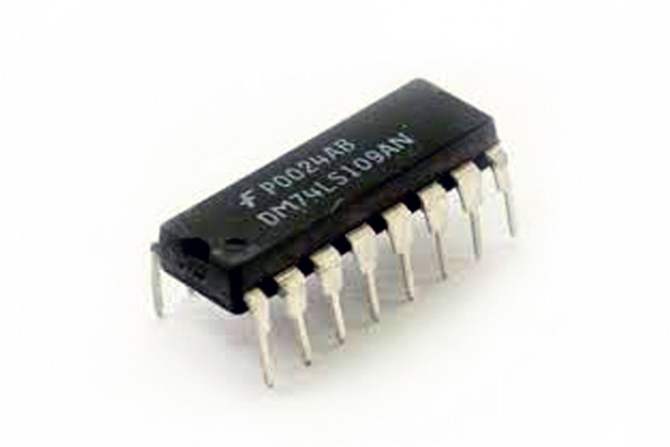
74LS109 Dual J-K Positive-edge-triggered Flip-Flop IC
Features and Specifications
Here are some important features and specifications of the 74LS109 IC.
- Positive Triggering edge
- Operating Voltage: 4.75V - 5.25V DC
- Frequency at normal voltage (Max): 35MHz
- Propagation delay (Max): 20ns
- High Output Current: 8 mA
- Low Output Current: 0.4 mA
Note: More technical information can be found in the 74LS109 Datasheet, linked at the bottom of this page.
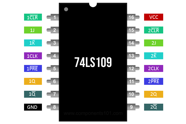
74LS109 Pinout Configuration
The IC consists of 16 pins in total, the table below can be referred to understand the pin configuration of the 74LS109 J-K Flip Flop IC.
|
Pin Number |
Pin Type |
Pin Description |
|
1 |
CLR1’ |
Active Low Clear Pin 1 |
|
2 |
J1 |
Input J1 |
|
3 |
K1’ |
Active Low Input 1 |
|
4 |
CLK |
Clock Input 1 |
|
5 |
1PRE’ |
Active low Preset pin 1 |
|
6 |
1Q |
Active high output 1 |
|
7 |
1Q’ |
Active low output 1 |
|
8 |
GND |
Ground |
|
9 |
2Q’ |
Active low output 2 |
|
10 |
2Q |
Active high output 2 |
|
11 |
2PRE’ |
Active low Preset pin 2 |
|
12 |
CLK2 |
Clock Input 2 |
|
13 |
K2’ |
Active low Input K2 |
|
14 |
J2 |
Input J2 |
|
15 |
CLR2’ |
Active low clear pin 2 |
|
16 |
VCC |
Positive supply voltage |
Working of the J-K Flip Flop IC
The JK flip-flops are the most efficient type of flip-flops and can be used in various applications. It was named after its inventor at Texas Instruments, Jack Kilby. This flip-flop has two inputs J and K along with two outputs Q and Q’. The flip-flop has a clock, clear, and a preset pin. Since 74LS109 has two flip-flops inside, both the flip-flops can be used individually.
Connecting the JK flip-flop IC is pretty easy, the IC is powered using a 5V supply, and the inputs(J, K) and outputs(Q, Q’) are supplied with the pins min/max supply voltages. As mentioned, the JK pins are the input pins that can be given a supply voltage and can be pulled down using a resistor to avoid any floating values. The reset pin should be grounded whenever we need to reset the flip flop. The Clock pin is responsible for changing the state of the output, a PWM signal can be provided to the clock pin and the outputs will change during the rising edge of the signal.
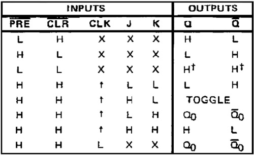
The truth table above can be referred to understand the output state with different input parameters.
Available Packages
PDIP, GDIP, PDSO
Alternatives
CD4027, 74HC107D, 74109, 74HC112D
Applications
Here are some of the applications of the JK Flip-flop IC.
- Counters
- Frequency dividers
- Registers


