CD4027 Dual Package JK Flip-Flop IC
The CD4027 is a CMOS based high voltage high speed Dual JK Flip-Flop package. The Flip-Flop could typically operate at a speed of 16MHz even at high voltages like 15V with a low noise margin of only 2.5V.
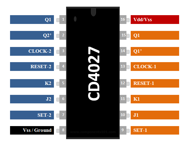
Pin Configuration
|
Pin Number |
Pin Name |
Description |
|
16 |
Vcc |
Powers the IC typically with 5V |
|
8 |
Ground |
Connected to the ground of the system |
|
JK Flip Flop – 1 / JK Flip Flop - 2 |
||
|
3,13 |
Clock-1/ Clock-2 |
These pins must be provided with clock pulse for the flip flop |
|
2,7 |
Reset-1 / Reset-2 |
When Preset is high the flip flop will set Q=1 and not Q=0 |
|
4, 12 |
Clear-1/Clear-2 |
When Clear is high the flip flop will set Q=0 and not Q=1 |
|
5, 11 |
K-1/ K-2 |
Input pin of the Flip Flop |
|
6, 10 |
J-1 / J-2 |
Another Input pin of the Flip Flop |
|
2,14 |
Q-1(bar) / Q-2 (bar) |
Inverted output pin of Flip Flop |
|
1,15 |
Q-1 / Q-2 |
Output Pin of the Flip Flop |
CD4027 Features
- Dual JK Flip Flop Package IC
- Operating Speed: 16MHz
- Operating Voltage: 5V, 10V, 15V
- Maximum Operating Voltage: 20V
- Input Rise/Fall time at 5V : 45us
- Minimum High Level Input Voltage: 2 V
- Maximum Low Level Input Voltage: 0.8 V
- Available in 14-pin PDIP, GDIP, PDSO packages
Note: Complete Technical Details can be found at the CD4027 datasheet attached at the end of this page.
CD4027 Equivalent
74HC76
Alternatives JK Flip-Flops
74HC73a, 74LS107, 4027B
Where to use CD4027 JK Flip-Flop
The CD4027 is a dual in-line JK flip flop IC. Meaning it has two JK flip flops inside it and each can be used individually based on our application. The term JK flip flop comes after its inventor Jack Kilby. The JK flip flops are considered to be the most efficient flip-flop and can be used for certain applications on its own. The flip-flops are also called as latching devices meaning it can remember one single bit of data and latch the output based on it, due to this property they are commonly used as shift registers, control registers, storage registers or where ever a small memory is required. More than one Flip Flop can be used in series to act as an EEPROM for holding small amount of data. The JK flip flop is considered to be more suitable for practical application because of its truth table that is the output of the flip flop will be stable for all types of inputs.
So if you are looking for a IC for latching purpose or to act as a small programmable memory for you project then this IC might be the right choice for you.
How to use CD4027 Flip Flop
As told earlier we have two JK flip flops in this IC, the IC is powered by +5V typically the minimum and maximum input and output voltage for the input (J,K) pins and the output (Q, Q bar) pins are discussed in the specifications above. The below circuit shows a typical sample connection for the JK flip-flop.
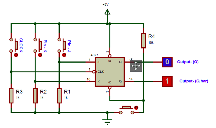
The J and K pins are the input pins for the Flip-Flop and the Q and Q bar pins are the output pins. Note that the input pins are pulled down to ground through a 1k resistor or less, this way we can avoid the pin in floating condition. That is the pin will held to ground when the button is not pressed and when the button is pressed the pin will be held to supply voltage.
The reset button should be pulled up through a 1K resistor and when grounded will reset the flip-flop. The clock signal for the JK flip-flop is responsible for changing the state of the output. The flip-flop will change its output only during the rising edge of the clock signal. The clock signal here is just a push button but can be type of pulse like a PWM signal. The output state of the flip flops can be determined form the truth table below.
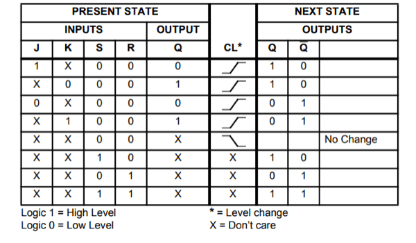
Normally during regular operation of the IC the reset pin will be set high and the clock pulse of known frequency will be supplied to the clock pin, then the value o J and K will be varied based on the input signals and the respective output will be obtained on the Q and Q bar pins. This region of operation in highlighted in red colour on the Truth table above.
Applications
- Shift Registers
- Memory/Control Registers
- EEPROM circuits
- Latching devices
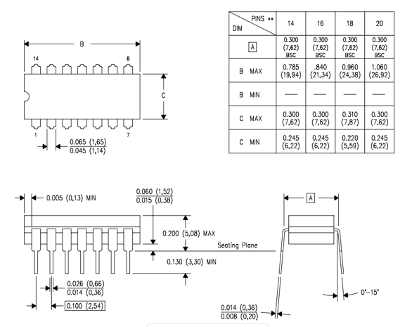
2D Model of 4027 (GDIP)