CD4067 16-Channel Analog Multiplexer/ Demultiplexer
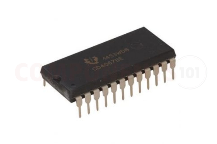
The CD4067 is a commonly used 16-channel analog multiplexer/demultiplexer. It has four digital inputs to control the 16-channel. It is used to switch one of 16 analog inputs to a single analog output, or multiple analog outputs can be controlled by a single digital output. The CD4067 is useful for expanding the number of analog inputs or outputs in electronic circuits. CD4067 provides Low ON resistance, high-speed switching and low power consumption. Applications of the CD4067 include data acquisition systems, instrumentation, audio signal routing, and analog signal processing. The CD4067 is available in various package options including PDIP, SOIC, and TSSOP, making it suitable for different PCB layouts and space constraints.
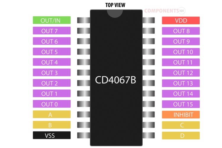
CD4067 Pinout Configuration
Here are the pinout details for CD4067.
| PIN NO | PIN NAME | DESCRIPTION |
| 1 | COM OUT/IN | Common out/in |
| 2 | CH 7 IN/OUT | Channel 7 in/out |
| 3 | CH 6 IN/OUT | Channel 6 in/out |
| 4 | CH 5 IN/OUT | Channel 5 in/out |
| 5 | CH 4 IN/OUT | Channel 4 in/out |
| 6 | CH 3 IN/OUT | Channel 3 in/out |
| 7 | CH 2 IN/OUT | Channel 2 in/out |
| 8 | CH 1 IN/OUT | Channel 1 in/out |
| 9 | CH 0 IN/OUT | Channel 0 in/out |
| 10 | A | Channel select A. |
| 11 | B | Channel select B. |
| 12 | VSS | Ground |
| 13 | D | Channel select D. |
| 14 | C | Channel select C. |
| 15 | INH | Disables all channels. |
| 16 | CH 15 IN/OUT | Channel 15 in/out |
| 17 | CH 14 IN/OUT | Channel 14 in/out |
| 18 | CH 13 IN/OUT | Channel 13 in/out |
| 19 | CH 12 IN/OUT | Channel 12 in/out |
| 20 | CH 11 IN/OUT | Channel 11 in/out |
| 21 | CH 10 IN/OUT | Channel 10 in/out |
| 22 | CH 9 IN/OUT | Channel 9 in/out |
| 23 | CH 8 IN/OUT | Channel 8 in/out |
| 24 | VDD | Positive power input |
Manufacturers of CD4067:
The CD4067 is originally manufactured by Texas Instruments. However, several other manufacturers also produce compatible versions of this IC. Some of the manufacturers are ON Semiconductor, NXP Semiconductor and Analog Devices.
CD4067 Equivalents
If you are looking for an equivalent or replacement for CD4067 there are no pin-to-pin compatible chips available, but you can consider the CD4097 from the same family. Keep in mind that, the CD4097 is a differential 8-channel multiplexer having three binary control inputs A, B, C and an inhibit input. The inputs permit the selection of one of eight pairs of switches.
CD4067 Alternatives
If you are looking for an alternative for CD4067 you can look at the other IC from these.
CD4051,74HC4051,74HC4067
Note: Complete technical details can be found in the CD4067 datasheet at this page’s end.
Features of CD4067
CD4067 CMOS Single 16-Channel Analog Multiplexer has the following key features:
- High Voltage Types (20V Rating)
- Low ON Resistance: 125Ω (typ) Over 15Vp-p Signal Input Range for VDD - VSS = 15V
- High OFF Resistance: Channel Leakage of ±10pA (typ) at VDD - VSS = 18V
- Matched Switch Characteristics: RON = 5Ω (typ) for VDD - VSS = 15V
- Very Low Quiescent Power Dissipation Under All Digital Control Input and Supply Conditions: 0.2µW (typ) at VDD - VSS = 10V
- Binary Address Decoding on Chip
- 5V, 10V and 15V Parametric Ratings
- 100% Tested for Quiescent Current at 20V
- Maximum Input Current of 1µA at 18V Over Full Package Temperature Range; 100nA at 18V and +25oC
- Standardized Symmetrical Output Characteristics
- Availability in different packages
CD4067 Functional Diagram
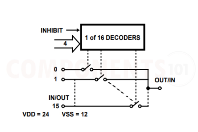
Here is the internal functional diagram of a CD4067. As you can see there is one common pin, which can be acted as an input or output, with 15 other inputs/outputs. The decoder block processes the control pins and switches on or off the corresponding input/output pin.
CD4067 Circuit Diagram
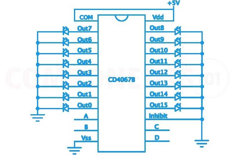
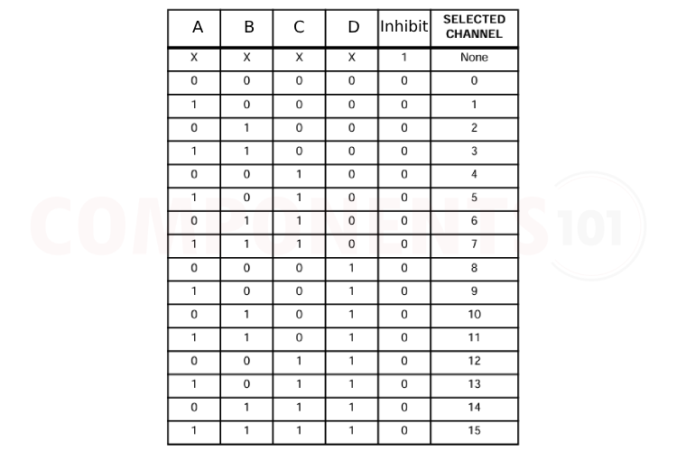
Here is a simple circuit built around the CD4067. For that, we have connected the common pin to the VDD. And LEDs are connected to all other output pins. Now by applying different signals to the Pins A, B, C and D, we can control all those LEDs. For controlling each output, please refer to the truth table below.
CD4067 Not Working?
- Circuit not working while using separate power supply signal and IC: In applications where separate power sources are used to drive VDD and the signal inputs, the VDD current capability should exceed VDD/RL (RL = effective external load). This provision avoids permanent current flow or clamp action on the VDD supply when power is applied or removed from the CD4067.
- Multiplexer is overlapping when switching from one address to another: When switching from one address to another, some of the ON periods of the channels of the multiplexers will overlap momentarily, which may be objectionable in certain applications. Also, when a channel is turned on or off by an address input, there is a momentary conductive path from the channel to VSS, which will dump some charge from any capacitor connected to the input or output of the channel. The inhibit input turning on a channel will similarly dump some charge to VSS.
- The circuit’s performance is not stable. There is a lot of noise introduced to the line: Ensure that the power supply to the CD4067 is stable and within the specified voltage range. Each VCC terminal should have a good bypass capacitor to prevent power disturbance. For devices with a single supply, a 0.1-μF bypass capacitor is recommended. The bypass capacitor should be installed as close to the power terminal as possible for best results.
Design Tips for CD4067
1. How to avoid VDD's current drawing?
In certain applications, the external load resistor current may include both VDD and signal-line components. To avoid drawing VDD current when switching current flows into the transmission gate inputs, the voltage drop across the bidirectional switch must not exceed 0.8 volts. No VDD current will flow through RL if the switch current flows into terminal 1 on the CD4067BMS, terminals 1 and 17 on the CD4097BMS.
2. How do we minimize noise while using CD4067?
Use bypass capacitors (typically 0.1 μF) between VDD and VSS and between VEE and VSS to stabilize the power supply and minimize noise.
3. Does the working of the circuit depend on the temperature?
The CD4067's performance can vary with temperature, so operate it within the specified temperature range for best results.
4. What are the design considerations when designing a PCB using CD4067?
Keep the analog signal paths short and avoid routing them close to noisy digital signals to minimize interference and signal degradation.
5. What is the difference between CD4067B, CD4067BE, CD4067BF, CD4067BP and CD4067BM?
CD4067B is the base part number, representing the general function of the IC. The other suffixes indicate different packages. The CD4067BE and CD4067BF both represent DIP packages, where the suffix E is for the plastic DIP package while the F is for the ceramic DIP package. The CD4067BP indicates the TSSOP package and CD4067BM indicates the SOIC package.
Applications of CD4067
- Analog and Digital Multiplexing and Demultiplexing
- A/D and D/A Conversion
- Signal Gating
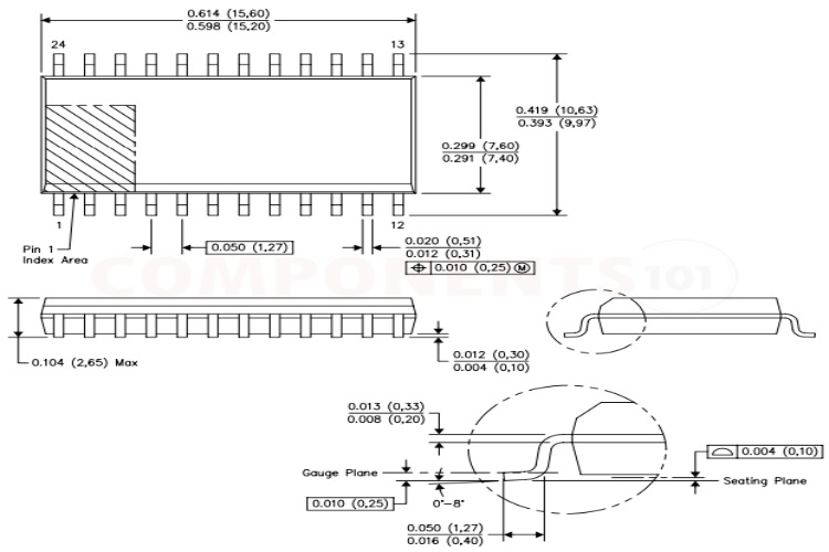
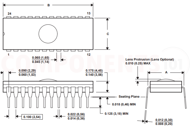
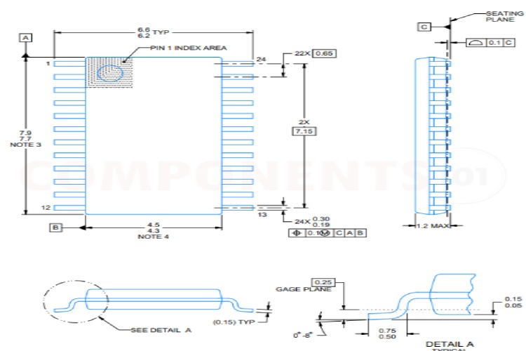
2D Model and Dimensions of CD4067
Here you can find the mechanical drawings of CD4067 along with its dimensions. The dimensions can be used to create custom footprints of the module and be used for PCB or CAD modelling.
DIP PACKAGE
TSSOP PACKAGE
PLASTIC SMALL OUTLINE