ADXL345 3-Axis Digital Accelerometer
The ADXL345 is an ultra-low power, small 3-Axis MEMS digital accelerometer. The ADXL345 offers a high resolution of 13-bit in its measurements at up to ±16g. It can also be interfaced with either SPI or I2C protocols. It measures the static acceleration as well as dynamic acceleration during a movement. As the name suggests, the ADXL345 has three axes of measurement. The sensitivity level of the chip can also be configured to either ±2g, ±4g, ±8g or ±16g. The lower range gives more resolution for slow movement, while the higher range is optimal for tracking high speed movements. The maximum voltage applied to the VS and VDD io pin should not exceed 3.3V.
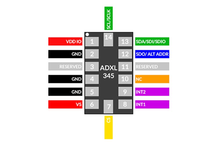
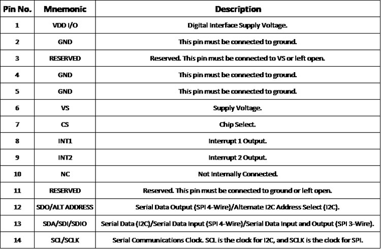
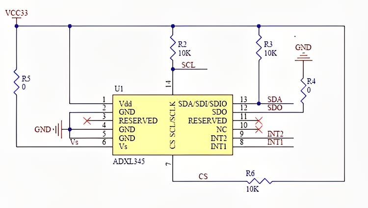
ADXL345 Pinout Configuration
Features
-
Ultralow power: as low as 23μA in measurement mode and 0.1μA in standby mode at VS = 2.5 V (typical)
-
Power consumption scales automatically with bandwidth
-
User-selectable resolution
-
Fixed 10-bit resolution.
-
Full resolution, where resolution increases with g range, up to 13-bit resolution at ±16 g (maintaining 4 mg/LSB scale factor in all g ranges)
-
-
Embedded memory management system with FIFO technology minimizes host processor load.
-
Single tap/double tap detection
-
Activity/inactivity monitoring
-
Free-fall detection
-
Supply voltage range: 2.0 V to 3.6 V
-
I/O voltage range: 1.7 V to VS
-
SPI (3- and 4-wire) and I2C digital interfaces
-
Flexible interrupt modes mappable to either interrupt pin
-
Measurement ranges selectable via serial command.
-
Bandwidth selectable via serial command
-
Wide temperature range (−40°C to +85°C)
-
10,000 g shock survival
-
Pb free/RoHS compliant
-
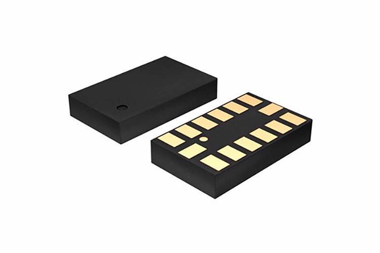
Small and thin: 3 mm × 5 mm × 1 mm LGA package
Note: Complete technical details can be found in the ADXL345 datasheet at this page’s end.
Alternative Accelerometer Chips: ADXL335, LIS3DH, MPU6050, AIS2IH, AIS2DW12
How To Use ADXL345?
The image below shows the typical schematics for ADXL345. In the schematics, we have choose I2C protocol for interface. You can also use SPI with small changes. The power inputs VDD IO and VS are connected to 3.3V. The SDO pin is grounded, and the chip select pin is pulled up to enable the chip. External pullups are added to the SCL and SDA lines for proper communication.
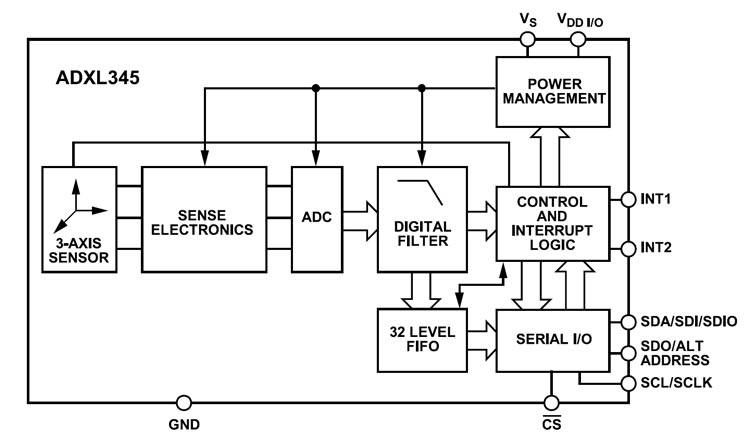
Functional Block Diagram
Applications
- Handsets
- Medical instrumentation
- Gaming and pointing devices.
- Industrial instrumentation
- Personal navigation devices
- Hard disk drive (HDD) protection
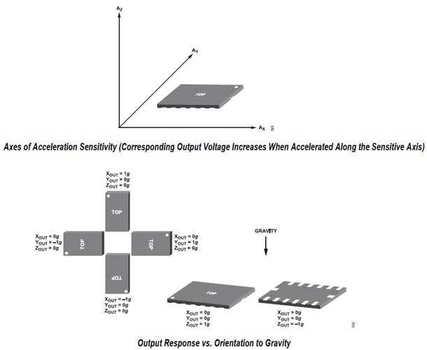
Axis of Acceleration Sensitivity
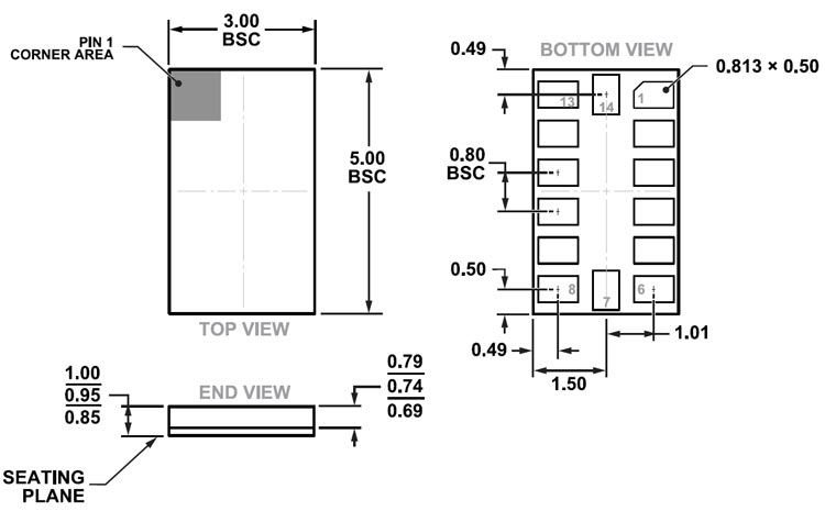
2D-Model and Dimensions