FGH40N60SMD Field Stop IGBT Pinout, Equivalent, Datasheet & Application Circuit
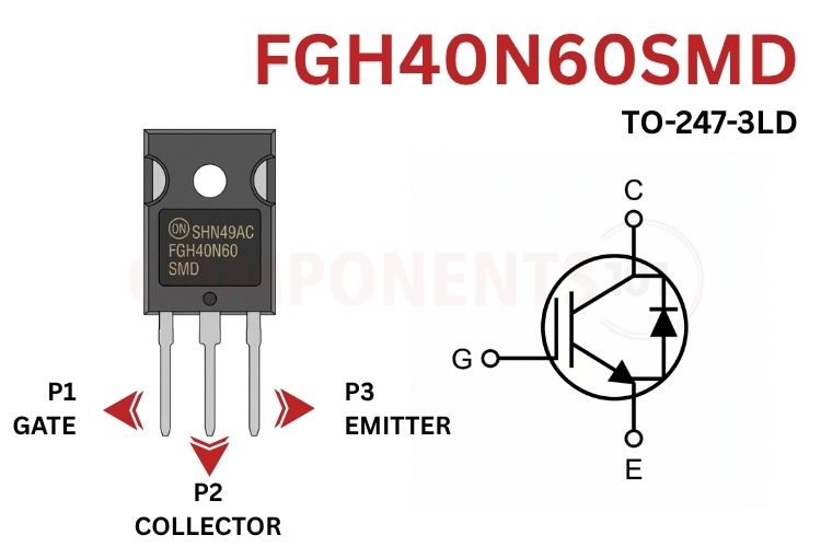
FGH40N60SMD Pinout Configuration
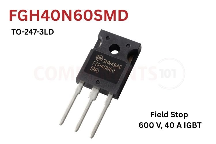
The FGH40N60SMD is an onsemi 600 V, 40 A field-stop (2nd generation) IGBT with a co-packaged anti-parallel diode in a TO-247-3LD package. The FGH40N60SMD Pinout follows the standard JEDEC TO-247-3LD 3-pin arrangement:
| Pin Number | Pin Name | Description |
| 1 | Gate (G) |
Voltage control terminal. Applying +15V relative to the Emitter switches the IGBT fully ON into low-saturation conduction. |
| 2 | Collector (C) | High-voltage power terminal connected to the positive switched load or high-voltage DC bus. Internally bonded to the metallic TO-247 mounting tab. |
| 3 | Emitter (E) | Power return terminal connected to high-voltage ground, negative DC rail, or low-side current sensing shunt. |
| Tab | Collector (C) | Metallic heatsink tab electrically bonded to Pin 2 Collector for maximum heat extraction to an external heatsink. |
*Note: Because the metal mounting heatsink tab is bonded directly to Pin 2 Collector, mounting the device onto a shared grounded chassis or common heatsink requires an electrical insulating pad (sil-pad or mica sheet with an insulating bushing) to prevent high-voltage shorts.
FGH40N60SMD Key Features & Specifications
- Transistor Type / Architecture: Field Stop 2nd Generation N-Channel IGBT with Co-Packaged Diode
- Collector-to-Emitter Voltage (VCES): 600V (at VGE = 0V, IC = 250 µA)
- Gate-to-Emitter Voltage (VGES): ±20V continuous (±30V transient)
- Continuous Collector Current (IC) at TC = 25°C: 80A
- Continuous Collector Current (IC) at TC = 100°C: 40A
- Pulsed Collector Current (ICM): 120A (pulse width limited by maximum junction temperature)
- Diode Continuous Forward Current (IF): 40A at TC = 25°C; 20A at TC = 100°C
- Diode Pulsed Forward Current (IFM): 120A
- Maximum Power Dissipation (PD): 349W at TC = 25°C; 174W at TC = 100°C
- Collector-to-Emitter Saturation Voltage (VCE(sat)): 1.9V typ, 2.4V max at VGE = 15V, IC = 40A, TC = 25°C (2.1V typ at TC = 175°C)
- Gate Threshold Voltage (VGE(th)): 3.5V min, 4.5V typ, 6.0V max at VCE = VGE, IC = 250 µA
- Input Capacitance (Cies): 1880 pF typ at VCE = 30V, VGE = 0V, f = 1.0 MHz
- Output Capacitance (Coes): 180 pF typ; Reverse Transfer Capacitance (Cres): 50 pF typ
- Total Gate Charge (Qg): 119 nC typ, 180 nC max at VCC = 400V, IC = 40A, VGE = 15V
- Gate-to-Emitter Charge (Qge): 13 nC typ; Gate-to-Collector Charge (Qgc): 58 nC typ
- Turn-On Delay Time (td(on)): 12 ns typ; Rise Time (tr): 20 ns typ (VCC = 400 V, IC = 40 A, RG = 6.0 Ω, VGE = 15 V)
- Turn-Off Delay Time (td(off)): 92 ns typ; Fall Time (tf): 13 ns typ
- Turn-On Switching Loss (Eon): 0.87 mJ typ; Turn-Off Switching Loss (Eoff): 0.26 mJ typ
- Total Switching Energy Loss (Ets): 1.13 mJ typ at TC = 25°C; 1.57 mJ typ at TC = 175°C
- Diode Forward Voltage Drop (VFM): 2.3V typ, 2.8V max at IF = 20A, TC = 25°C (1.67V typ at TC = 175°C)
- Operating Junction Temperature (TJ): -55°C to +175°C
- Package Type: TO-247-3LD (Through-Hole Power Package, Case 340CK)
*Note: Complete Technical Details can be found in the FGH40N60SMD datasheet given at the end of this page.
FGH40N60SMD Equivalent & Alternative Components
A true FGH40N60SMD equivalent should match the 600 V class, a similar 40 A rating, the TO-247 package, the G-C-E pin order and a comparable gate threshold and switching speed. The parts below are grouped by how safely they can replace it.
| Equivalent Part | Polarity / Type | Key Ratings | Description & Compatibility Notes |
| FGH60N60SMD | IGBT + Diode | 600V, 60A (100°C), VCE(sat)=1.9V, TO-247 | Higher current 60A variant from the same onsemi Field Stop family; drop-in power upgrade. |
| IKW40N120H3 | IGBT + Diode | 1200V, 40A (100°C), VCE(sat)=2.05V, TO-247 | Infineon HighSpeed 3 IGBT; higher 1200V rating for 400V/480V 3-phase industrial grids. |
| IKW50N60T | IGBT + Diode | 600V, 50A (100°C), VCE(sat)=1.5V, TO-247 | Infineon TrenchStop 600V 50A alternative with ultra-low forward saturation drop. |
| STGW40H120DF | IGBT + Diode | 1200V, 40A (100°C), VCE(sat)=2.1V, TO-247 | STMicroelectronics Trench Gate Field-Stop IGBT for high-voltage industrial inverters. |
| RJH60F7DPQ | IGBT + Diode | 600V, 90A (100°C), VCE(sat)=1.75V, TO-247 | Renesas ultra-fast trench IGBT commonly used in Asian inverter welders. |
| IRG4PC50UD | IGBT + Diode | 600V, 27A (100°C), UltraFast, TO-247 | Classic International Rectifier legacy IGBT with integrated HEXFRED diode. |
Brief Description of the FGH40N60SMD IGBT
The FGH40N60SMD is built on onsemi's proprietary 2nd-generation Field Stop trench technology, which optimizes the carrier lifetime and electric field distribution across the silicon drift region. This architecture significantly narrows the active base width, simultaneously minimizing on-state conduction voltage (VCE(sat) = 1.9V) and curtailing the inductive turn-off current tail that historically constrained older non-punch-through (NPT) IGBTs.
1. Gate Drive Voltage: Use a +15V gate-to-emitter drive for efficient conduction. Keep the voltage within the ±20V absolute maximum rating to prevent gate damage.
2. Integrated Fast-Recovery Diode: The built-in anti-parallel diode has a 36 ns reverse recovery time and 46.8 nC recovery charge, reducing the need for external freewheeling diodes in bridge and boost circuits.
3. Parallel Operation: Its positive temperature coefficient at higher currents can improve current sharing between parallel IGBTs, provided the gate drive and layout are properly designed.
4. Thermal Management: With a junction-to-case thermal resistance of 0.43 °C/W, effective heatsinking is essential. At 30 A and 1.9 V saturation voltage, conduction losses reach approximately 57 W, requiring a suitable heatsink and potentially forced-air cooling.
FGH40N60SMD Datasheet
The complete original manufacturer electrical characteristics, thermal impedance curves, switching energy charts, and safe operating area (SOA) waveforms are available in the official onsemi FGH40N60SMD Datasheet.
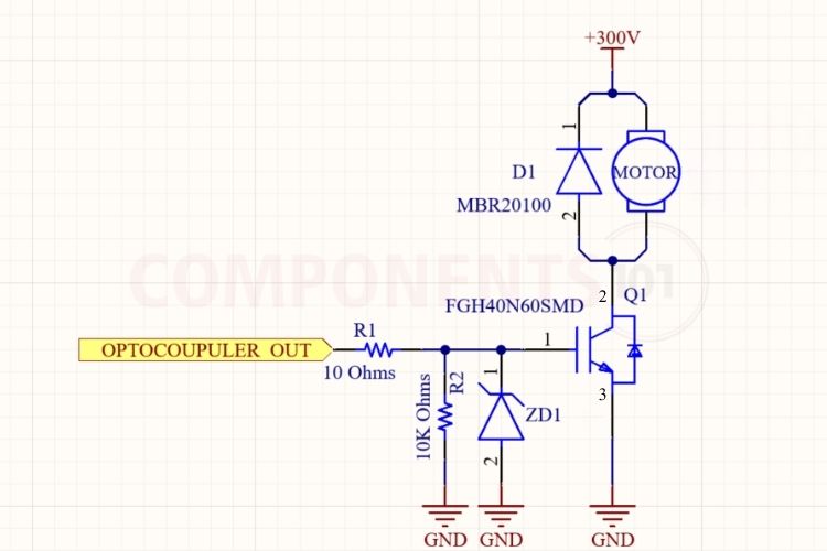
FGH40N60SMD Circuit Diagram: High-Voltage DC Load Switching
The schematic below demonstrates a straightforward, practical high-voltage DC load switching circuit using the FGH40N60SMD as a low-side solid-state power switch. An optically isolated gate driver IC (TLP250 or FOD3180) bridges the low-voltage microcontroller logic domain with the high-voltage 300V DC power domain. This FGH40N60SMD circuit diagram shows a practical low-side solid-state switch for a high-voltage DC load.
How to Use the FGH40N60SMD in a Circuit
- The load is connected to the positive DC bus in series with the collector of the IGBT whereas the emitter goes back to the DC bus negative terminal.
- The microcontroller drives the LED side of the optocoupler gate driver while keeping the logic ground isolated from the ground of the power circuit.
- The output of the optocoupler gate driver which is supplied from 15V line, charges the gate of the IGBT via a series resistor thereby making the IGBT turn ON.
- The IGBT switches OFF when the logic signal goes low, and the optocoupler gate driver takes the gate of the IGBT to the emitter voltage.
- In a case of inductive loads, the current of the load is allowed to travel under the condition that the voltage of the collector does not exceed 600V with the help of either clamp or freewheeling diode.
FGH40N60SMD Applications
Lists the following target applications for this FGH40N60SMD IGBT.
- Inverter Arc Welding Machines (MMA / TIG / MIG): Primary high-frequency (20 kHz to 50 kHz) half-bridge and full-bridge power switching stage converting rectified mains power into 160A–200A welding currents.
- Solar Central & String Inverters: High-efficiency DC-AC bridge inverters and high-voltage MPPT boost stages in residential and commercial photovoltaic installations.
- Uninterruptible Power Supplies (UPS): High-power DC-to-AC pure sine wave inverter stages for telecom and data center backup power systems.
- Active Power Factor Correction (PFC): High-voltage continuous conduction mode (CCM) boost converters in industrial switched-mode power supplies.
- Industrial Induction Heating & Cooktops: Resonant half-bridge inverter stages switching high-frequency AC current through induction work coils.
- Variable Frequency Motor Drives (VFD): Three-phase inverter bridge output stages driving industrial AC induction and brushless DC motors.
2D Model and Component Dimensions
For PCB footprint layout designers using KiCad, Altium Designer, Eagle, or EasyEDA, the mechanical dimensions for the standard TO-247-3LD (onsemi Case 340CK) package are detailed below:
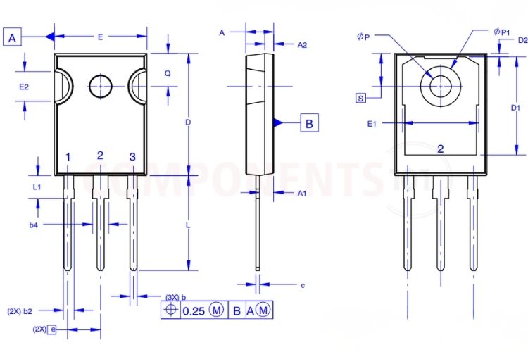
| Parameter Symbol & Description | Minimum (mm) | Nominal (mm) | Maximum (mm) |
| A (Total Package Thickness / Depth) | 4.58 | 4.70 | 4.82 |
| A1 (Lead Offset / Seating Plane Distance) | 2.20 | 2.40 | 2.60 |
| A2 (Base Plastic Thickness) | 1.40 | 1.50 | 1.60 |
| b (Lead Width, 3 Leads) | 1.17 | 1.26 | 1.35 |
| b2 (Upper Lead Shoulder Width, 2 Leads) | 1.53 | 1.65 | 1.77 |
| b4 (Center Lead Shoulder Width) | 2.42 | 2.54 | 2.66 |
| c (Lead Thickness) | 0.51 | 0.61 | 0.71 |
| D (Total Body Length / Height) | 20.32 | 20.57 | 20.82 |
| D1 (Exposed Heatsink Tab Height) | 13.08 min | - | - |
| D2 (Tab Notch Reference Height) | 0.51 | 0.93 | 1.35 |
| E (Total Molded Body Width) | 15.37 | 15.62 | 15.87 |
| E1 (Mounting Heatsink Tab Width) | 12.81 min | - | - |
| E2 (Upper Molded Notch Width) | 4.96 | 5.08 | 5.20 |
| e (Lead Pitch / Pin Spacing) | - | 5.56 BSC | - |
| L (Lead Length Below Seating Plane) | 15.75 | 16.00 | 16.25 |
| L1 (Lead Shoulder Length) | 3.69 | 3.81 | 3.93 |
| P (Mounting Hole Diameter øP) | 3.51 | 3.58 | 3.65 |
| P1 (Upper Mounting Hole Recess Diameter) | 6.60 | 6.80 | 7.00 |
| Q (Mounting Hole Center to Tab Top) | 5.34 | 5.46 | 5.58 |
| S (Mounting Hole Center to Body Edge) | 5.34 | 5.46 | 5.58 |
Safety warning: A 300 V DC bus can cause severe injury. Use an isolated supply, discharge bulk capacitors before touching the board, keep the heatsink insulated from the Collector and test first at a low bus voltage with current limiting.