BAT54S Dual Schottky Barrier Diode Pinout, Specifications, Marking Code & Datasheet
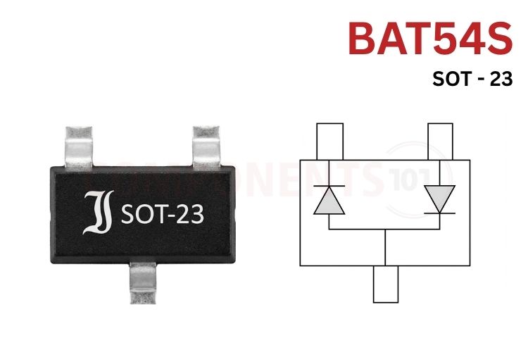
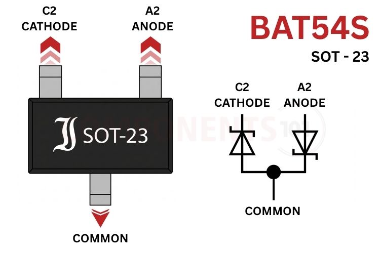
BAT54S Pinout Configuration
The BAT54S integrates two Schottky diodes connected in series inside a standard 3-terminal SOT-23 package. The terminal designations, internal connections, and functional descriptions are outlined below:
| Pin Number | Pin Name | Description |
| 1 | Anode 1 (A1) | Anode terminal of the lower Schottky diode (D1). Typically tied to Circuit Ground (GND / 0V) for negative undershoot clamping. |
| 2 | Cathode 2 (C2) | Cathode terminal of the upper Schottky diode (D2). Typically connected to the positive supply rail (VDD / VCC, +3.3V or +5.0V) for overvoltage clamping. |
| 3 | Common (Cathode 1 / Anode 2) | Common center-tap node connecting the cathode of Diode 1 and the anode of Diode 2. Connects directly to the protected I/O or analog signal line. |
BAT54S SOT-23 SMD Marking Code
Because the SOT-23 package measures only 2.9 mm by 1.3 mm, manufacturers print shorthand alphanumeric SMD top marking codes on the plastic encapsulation rather than the full part number:
| Marking Code | Manufacturer / Grade | Package | Notes / Identification |
| KL4 | Diodes Inc / JCET / LCSC | SOT-23 | Most common global marking; standard JLCPCB Basic Component for contract PCB assembly |
| L44 | Nexperia / Diotec / Vishay | SOT-23 | Standard industrial and AEC-Q101 qualified high-reliability grade |
| KL1 | Diotec Semiconductor | SOT-23 | Commercial grade designation (BAT54S-C) |
| B44 | onsemi (Fairchild) | SOT-23 | Automotive and industrial production line marking |
| WV4 | STMicroelectronics | SOT-23 | High-volume European automotive and industrial grade |
*Note: Suffix characters, vertical dots, or underlined characters adjacent to the primary marking code indicate factory manufacturing lot numbers, year, and production week trace codes.
BAT54S Key Features & Specifications
The electrical specifications listed below represent benchmark parameters across primary manufacturers (Diotec Semiconductor, Nexperia, Diodes Incorporated, and onsemi) at an ambient operating temperature of 25°C:
- Diode Configuration: Dual Series-Connected Schottky Barrier Diodes (Common Center Tap)
- Continuous Reverse Voltage (VR): 30V
- Repetitive Peak Reverse Voltage (VRRM): 30V
- Continuous Forward Current (IF / IFAV): 200 mA (DC)
- Repetitive Peak Forward Current (IFRM): 300 mA (tp ≤ 1 s, duty cycle ≤ 50%)
- Non-Repetitive Peak Forward Surge Current (IFSM): 600 mA (Half-sine pulse, tp ≤ 1 s)
- Forward Voltage Drop (VF @ 25°C):
at IF = 0.1 mA: < 0.24V (typical 0.22V)
at IF = 1.0 mA: < 0.32V (typical 0.29V)
at IF = 10 mA: < 0.40V (typical 0.35V)
at IF = 30 mA: < 0.50V (typical 0.41V)
at IF = 100 mA: < 1.00V (typical 0.80V)
- Reverse Leakage Current (IR): < 2.0 μA (at VR = 25V, 25°C; typical 0.5 μA)
- Total Junction Capacitance (CT / CJ): 10 pF maximum (typical 7.0 pF at VR = 0V, f = 1 MHz)
- Total Device Power Dissipation (PD / Ptot): 290 mW (Diotec industrial) / 200 mW (Diotec commercial) / 225 mW to 250 mW (standard SOT-23)
- Package Designation: SOT-23 / TO-236AB (3-Lead Surface Mount Device)
*Note: Complete Technical Details can be found in the BAT54S datasheet given at the end of this page.
BAT54S Equivalent & Alternative Components
When selecting replacements or variants within the BAT54 semiconductor family, engineers must verify terminal configurations, breakdown voltage ratings, and forward conduction characteristics:
| Part Number | Configuration | Package | Key Ratings (VR, IF, VF) | Primary Application & Functional Difference |
| BAS70-04 | Series Pair | SOT-23 | 70V, 70 mA, VF=0.41V | Higher-voltage Schottky series pair (marking 74) for 24V industrial signalling. |
| 1PS76SB40 | Series Pair | SOT-23 | 40V, 120 mA, VF=0.38V | Ultra-low leakage Schottky series pair optimised for battery-powered instruments. |
| BAV99 | Series Pair | SOT-23 | 70V, 215 mA, VF=0.72V | Standard silicon PN junction series pair (marking A7); higher VF, but handles higher voltage. |
| BAT54C | Common Cathode | SOT-23 | 30V, 200 mA, VF=0.32V | Dual common cathode pair (marking KL3 / L43); used for diode-OR power rail multiplexing. |
| BAT54A | Common Anode | SOT-23 | 30V, 200 mA, VF=0.32V | Dual common anode pair (marking KL2 / L42); used for ground-referenced signal steering. |
| BAT54 | Single Diode | SOT-23 | 30V, 200 mA, VF=0.32V | Single Schottky diode (marking KL1 / L4); pin 1 anode, pin 3 cathode, pin 2 unused. |
| 1N5819 / BAT43 | Single (THT) | DO-41 / DO-35 | 30V-40V, 200mA-1A | Through-hole Schottky diodes wired in series on solderless breadboards for prototyping. |
Brief Technical Description of BAT54S
The BAT54S is built around planar Schottky barrier technology, utilizing a metal-to-silicon semiconductor junction rather than a standard silicon P-N junction. Because conduction occurs predominantly via majority carriers (electrons in N-type silicon), there is virtually zero stored minority carrier charge in the depletion region. This enables three decisive operating advantages in embedded circuitry:
1. Ultra-Low Forward Voltage Drop: At micro-currents typical of signal monitoring (0.1 mA to 1.0 mA), the forward voltage drop is only 0.22V to 0.32V, compared to 0.65V to 0.75V for standard silicon diodes.
2. Nanosecond Switching Speed: The reverse recovery time is negligible (trr < 5.0 ns), allowing the device to clamp ultra-fast ESD spikes and high-frequency ringing without transient overshoot.
3. Minimal Capacitive Loading: With a total junction capacitance of under 10 pF (typically 7 pF at 0V reverse bias), the BAT54S introduces negligible low-pass attenuation on high-speed digital communications buses (such as 10 MHz SPI, 400 kHz I2C, and high-baud UART) and high-impedance analog sensor lines.
BAT54S Datasheet
Download the manufacturer technical BAT54S datasheet for the BAT54S dual Schottky barrier diode
How to Use the BAT54S in a Circuit
The primary and most celebrated circuit configuration for the BAT54S is as a dual-rail overvoltage and negative undershoot clamping protector for microcontroller GPIO and ADC analog inputs.
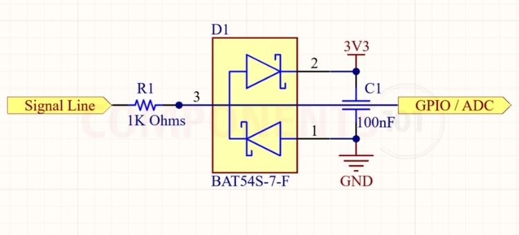
Detailed Circuit Operation & Component Selection
1. Current-Limiting Resistor (R1 = 1 kΩ):
An external input signal line (from an off-board analog sensor, push button, rotary encoder, or serial bus) connects to the circuit via a series current-limiting resistor. If an accidental overvoltage fault occurs (for example, +15V injected into a 3.3V system), R1 drops the excess voltage and restricts the peak current flowing through the clamping diodes:
I_FAULT = (15V - (3.3V + 0.32V)) / 1000 Ω = 11.38 mA
Because 11.38 mA is far below the continuous 200 mA rating of the BAT54S, the diode operates well within its thermal safe operating area indefinitely. For high-speed digital lines (such as SPI or UART), R1 is typically reduced to 100 Ω to 330 Ω to prevent RC rise-time degradation.
2. Positive Overvoltage Clamping (Upper Diode, Pin 3 to Pin 2):
Pin 2 of the BAT54S connects directly to the positive power supply rail (VDD / VCC, such as +3.3V or +5.0V), while Pin 3 connects to the protected signal node. Under normal operating conditions (Vin between 0V and 3.3V), diode D2 is reverse-biased with less than 1 μA of leakage current, having zero impact on signal measurement.
If an overvoltage transient or electrostatic discharge causes Vin to rise above `VCC + VF` (approximately `3.3V + 0.32V = 3.62V`), diode D2 immediately forward-biases and steers the excess surge energy directly into the VCC power supply rail. The voltage entering the microcontroller GPIO pin is strictly clamped to 3.62V, safely below the maximum absolute rating of the MCU (typically VDD + 0.3V to VDD + 0.5V).
3. Negative Undershoot Clamping (Lower Diode, Pin 1 to Pin 3):
Pin 1 of the BAT54S connects to Circuit Ground (GND / 0V), while Pin 3 connects to the protected signal node. When long external signal wires experience inductive ringing, inductive kickback, or ground bounces that swing below ground, the signal voltage drops negative.
When Vin falls below `-VF` (approximately `-0.32V`), diode D1 forward-biases from ground, clamping the signal line to `-0.32V`. This prevents the microcontroller's internal parasitic substrate NPN/PNP structures from turning ON, eliminating destructive CMOS latch-up conditions.
Applications
- Microcontroller I/O Protection: Clamping GPIO, interrupt, and reset pins on ESP32, STM32, Arduino, Microchip PIC, and Raspberry Pi boards against field wiring errors and static discharge.
- Analog-to-Digital Converter (ADC) Front-Ends: Protecting precision 12-bit, 16-bit, and 24-bit ADC input channels against transducer overvoltage without introducing parasitic leakage errors.
- Industrial Communication Buses: Signal rail clamping on RS-485, CAN bus, I2C, SPI, and UART lines routed between external equipment or long wiring harnesses.
- Rotary Encoders and External Pushbuttons: Suppressing inductive ringing and contact bounce spikes from mechanical switches, limit switches, and motor feedback sensors.
- Reverse Polarity and Voltage Steering: Low-loss signal steering, diode logic gates, and reverse polarity clamping in low-voltage battery-operated devices.
- Appliance & Automotive Control Boards: Input conditioning for washing machine sensors, automotive dashboard controllers, and smart energy meters.
2D Model and Component Dimensions
For engineers creating custom footprints or verifying solder land patterns in CAD packages (KiCad, Altium Designer, Autodesk Eagle, EasyEDA), the physical dimensions for the standard SOT-23 (TO-236AB) package are provided below:
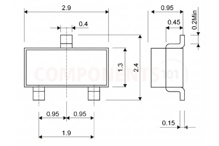
The table below summarizes the mechanical dimensions matching the official manufacturer package outline:
| Dimension Parameter | Symbol | Min (mm) | Typ (mm) | Max (mm) |
| Package Body Length | D | 2.80 | 2.90 | 3.00 |
| Total Width (Including Leads) | E | 2.20 | 2.40 | 2.60 |
| Package Body Width | E1 | 1.20 | 1.30 | 1.40 |
| Package Body Height / Thickness | A | 0.85 | 0.95 | 1.05 |
| Total Height (Including Standoff) | A1 | 0.90 | 1.10 | 1.20 |
| Lead Width (Pins 1, 2, 3) | b | 0.35 | 0.40 | 0.50 |
| Lead Pitch (Pin 1 to Pin 2 Center) | e | 1.70 | 1.90 | 2.10 |
| Lead Offset (Center to Pin 1/2) | e1 | 0.85 | 0.95 | 1.05 |
| Lead Frame Thickness | c | 0.08 | 0.14 | 0.20 |
| Lead Foot Length (Contact Area) | L | 0.20 | 0.35 | 0.55 |
| Lead Standoff / Seating Height | L1 | 0.20 | 0.25 | 0.35 |