AO3401A P-Channel MOSFET Pinout, Specifications, Marking Code & Datasheet
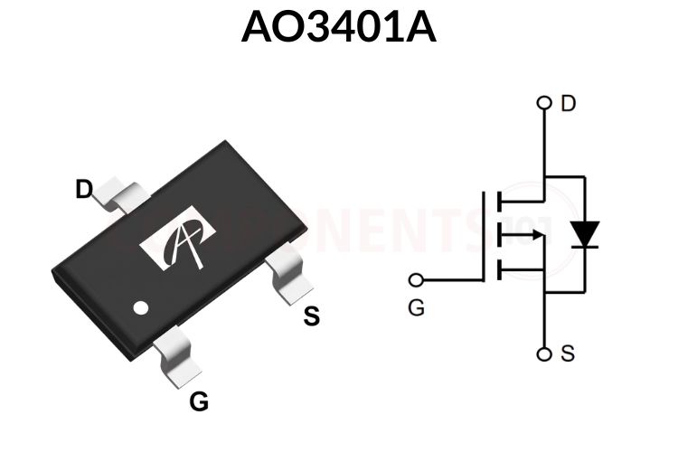
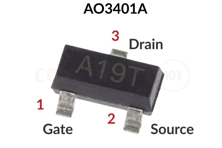
AO3401A Pinout Configuration
The AO3401A pinout follows the standard SOT-23 layout for P-channel MOSFETs.
| Pin Number | Pin Name | Description |
| 1 | Gate (G) | Controls MOSFET conduction. Applying a negative voltage relative to the source turns the channel ON. |
| 2 | Source (S) | Current enters through the source terminal. Connected to the positive supply rail in high-side switches. |
| 3 | Drain (D) | Current flows out through the drain terminal to the load's positive terminal. |
AO3401A SOT-23 SMD Marking Code (A19T MOSFET)
The AO3401A is a -30V, -4A P-channel enhancement-mode MOSFET in a SOT-23 package, made by Alpha & Omega Semiconductor (AOS). Because SOT-23 packages are extremely small (2.9 mm × 1.3 mm), manufacturers print shorthand SMD marking codes rather than the full part number:
| Marking Code | Manufacturer / Variant | Package | Notes |
| A19T | Alpha & Omega Semiconductor (AOS) | SOT-23 | Most common official marking code worldwide. |
| X1DV | Alternate / OEM Variant | SOT-23 | Common marking code found on JLCPCB / LCSC basic stock. |
| 3401 | Second-source Clone | SOT-23 | Generic Chinese second-source fab marking. |
*Note: Suffix characters or vertical bars next to the marking code indicate the production year, week, or fab lot trace code.
AO3401A Key Features & Specifications
- Transistor Polarity: P-Channel Enhancement Mode
- Drain-Source Voltage (VDS): -30V
- Continuous Drain Current (ID): -4.0A (@ VGS = -10V, TA = 25°C); -3.2A (@ TA = 70°C)
- Pulsed Drain Current (IDM): -30A
- Gate-Source Voltage (VGS): ±12V
- Low On-State Resistance (RDS(on)):
1. < 50 mΩ @ VGS = -10V
2. < 60 mΩ @ VGS = -4.5V
3. < 85 mΩ @ VGS = -2.5V
- Gate Threshold Voltage (VGS(th)): -0.5V (Min) to -1.3V (Max) (Fully enhanced at -2.5V and -3.3V logic)
- Total Gate Charge (Qg): 7 nC (Typ @ -4.5V); 14 nC (Typ @ -10V)
- Maximum Power Dissipation (PD): 1.4W (TA = 25°C); 0.9W (TA = 70°C)
- Operating Junction & Storage Temperature: -55°C to +150°C
- Package Type: SOT-23-3L (Surface Mount)
AO3401A Datasheet
The official AO3401A datasheet (PDF) from Alpha & Omega Semiconductor lists the full electrical characteristics, thermal data, safe operating area and package drawing. The values on this page are taken from that datasheet. Manufacturers revise datasheets, so check the latest revision before finalising a design.
*Note: Complete Technical Details can be found in the AO3401A datasheet given at the end of this page.
AO3401A Equivalent & Alternative MOSFETs
| Equivalent Part | Polarity | Key Ratings | Description & Features |
| AO3400A | N-Channel | 30V / 5.7A / 32 mΩ | Direct complementary N-Channel pair. Ideal for low-side switching and H-bridges. |
| SI2301 / SI2301CDS | P-Channel | -20V / -2.8A / 110 mΩ | Widely available low-voltage SMD P-channel MOSFET in SOT-23. |
| IRLML6402 | P-Channel | -20V / -3.7A / 65 mΩ | International Rectifier logic-level miniature P-MOSFET (Micro3). |
| DMG3415U | P-Channel | -20V / -4.0A / 42 mΩ | High-current logic-level P-channel substitute from Diodes Inc. (SOT-23). |
| BSS84 | P-Channel | -50V / -130mA / 10 Ω | Small-signal P-channel switching substitute only (low current loads). |
| IRF4905 | P-Channel | -55V / -74A / 20 mΩ | Through-hole TO-220AB high-power alternative for heavy prototyping. |
What Is the AO3401A MOSFET and How Does It Work?
The AO3401A is a compact SOT-23 P-channel MOSFET. In electronic designs, P-channel MOSFETs are preferred whenever a load must remain connected directly to system ground, and switching must occur on the positive supply rail (high-side switching).
Unlike N-channel MOSFETs, which require their gate voltage to be driven higher than the supply rail (requiring a charge pump or bootstrap capacitor in high-side configurations), a P-channel MOSFET turns ON simply by pulling its gate LOW relative to its source terminal.
The AO3401A is optimized as a sub-logic-level device with a maximum threshold voltage (VGS(th)) of only -1.3V. When the gate is pulled to ground in a 3.3V or 5V system, the effective VGS is -3.3V or -5V, driving the channel into full saturation with minimal on-resistance. This allows it to pass 2A to 3A of continuous DC with virtually zero voltage drop and no heatsink.
How to Use the AO3401A in a Circuit
The AO3401A is primarily used for high-side load switching and Ideal Reverse-Polarity Protection Circuits.
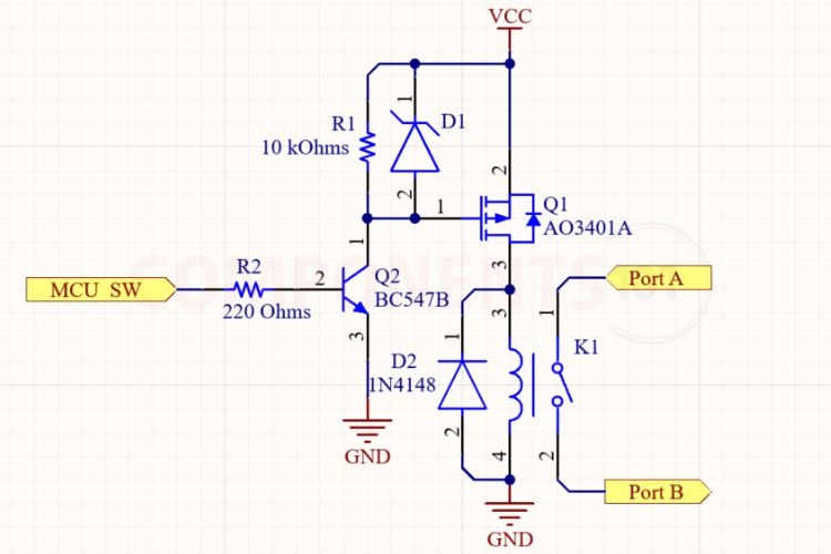
Circuit Operation & Component Selection
1. High-Side Load Switching with Microcontroller:
When switching supply voltages higher than the microcontroller logic level (such as 5V, 9V, or 12V), a small NPN transistor (such as a 2N3904, BC547, or MMBT3904) is used to pull the AO3401A gate to ground without exposing the MCU GPIO pin to higher rail voltages.
When the MCU GPIO output is LOW, the NPN transistor is OFF. A 10 kΩ gate pull-up resistor (R_PULLUP) tied between Source (VIN) and Gate holds VGS at 0V, keeping the AO3401A solidly OFF.
When the MCU GPIO pin goes HIGH, the NPN transistor turns ON and pulls the AO3401A gate toward ground. This creates a negative VGS, turning the AO3401A ON and powering the load connected to the drain.
2. Gate-to-Source Pull-Up Resistor (R_PULLUP):
A 10 kΩ to 100 kΩ pull-up resistor connected between Source and Gate is mandatory. It ensures that whenever the control signal is floating, disconnected, or during microcontroller boot, the gate remains tied to the source voltage (VGS = 0V), preventing accidental turn-on.
3. Gate Protection Zener (For VIN > 10V):
Because the maximum gate-to-source rating of the AO3401A is ±12V, operating from supply rails above 10V (such as 12V or 24V) requires a resistor divider or a 10V Zener diode placed across Gate and Source to clamp VGS within safe absolute limits.
4. Reverse Polarity Protection:
By connecting Source to the load side and Drain to the positive power input, with Gate tied to ground through a resistor, the AO3401A acts as an ideal low-loss diode. In normal polarity, current initially flows through the internal body diode, creating a negative VGS that fully enhances the channel, bypassing the diode drop. If power is accidentally reversed, VGS becomes positive, permanently locking the MOSFET OFF and saving downstream electronics.
Applications
- High-Side Power Distribution: Power gating subsystems, sensors, and GPS modules in battery-powered IoT devices.
- Reverse Battery Polarity Protection: Low-loss replacement for Schottky diodes in handheld gadgets and USB power inputs.
- H-Bridge High-Side Switches: Paired with AO3400A N-channel MOSFETs for bidirectional DC motor and actuator control.
- Li-Ion Battery Management (BMS): High-side battery disconnect and over-discharge cut-off switches.
- Display and Backlight Control: Power rail switching for OLED displays and LED indicator arrays.
- USB Port Power Switching: Over-current and power distribution control in single-board computers and hubs.
2D Model and Component Dimensions
For engineers designing a custom PCB or adding the AO3401A footprint to CAD tools (KiCad, Altium, Eagle, EasyEDA), the physical dimensions for the standard SOT-23-3L package are given below:
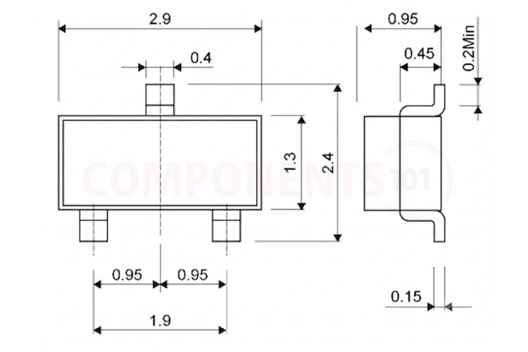
| Parameter | Min (mm) | Typ (mm) | Max (mm) |
| Body Length (D) | 2.80 | 2.90 | 3.04 |
| Total Width (E) | 2.10 | 2.30 | 2.64 |
| Body Width (E1) | 1.20 | 1.30 | 1.40 |
| Total Height (A) | 0.89 | 1.00 | 1.14 |
| Lead Pitch (e) | - | 1.90 (typ) | - |
| Lead Width (b) | 0.30 | 0.40 | 0.50 |