L4941-5V 1A Low Voltage Drop Regulator
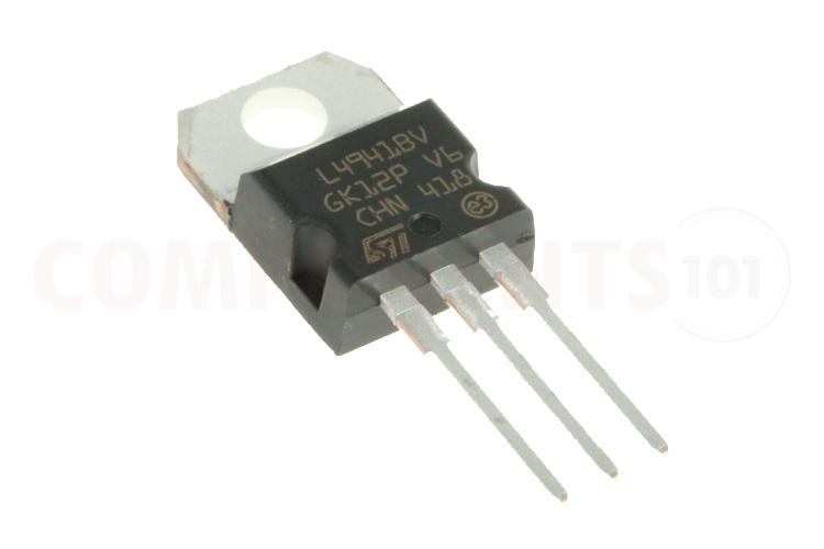
The L4941 is a 5V low dropout positive voltage regulator. It can regulate the output voltage even when the input voltage is only slightly higher than the output voltage. This is beneficial in battery-operated systems where maximizing battery life is crucial. This IC has only three terminals, which makes this IC, simple to use in circuits. It has a wide input voltage of up to 30V and it can deliver up to 1A output current. Even with the maximum current of 1A, the voltage drop across the regulator is only 450mV. This small IC integrates internal current limiting, Anti saturation circuit, thermal shut-down and safe area protection. The L4941 is commonly used in applications such as automotive electronics, consumer electronics, and other systems requiring a stable and regulated voltage supply. The L4941 is available in both TO-220 and DPAK packages.
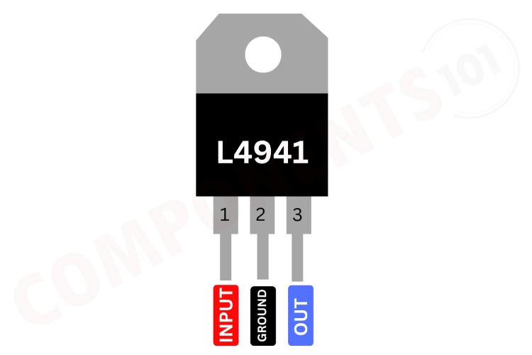
L4941 Pinout Configuration
Here are the pinout details for L4941.
| PIN | NAME | FUNCTION |
| 1 | INPUT | Positive Input voltage |
| 2 | GND | Ground. |
| 3 | OUT | Positive 5V output |
Features of L4941
L4941 5volt LDO has the following key features:
- Low dropout voltage (450mV typ. at 1A)
- Wide input voltage range
- Simple three-pin design
- Very low quiescent current
- Thermal shutdown
- Short circuit protection
- Reverse polarity protection
Manufacturers of L4941:
The L4941 is manufactured by STMicroelectronics. There are no alternative manufacturers for the same part number as of the date of writing this article.
L4941 Equivalents
If you are looking for an equivalent or replacement for L4941, you can use LM7805 which pin to pin compatible with the L4941, but keep in mind that the LM7805 has a higher voltage drop.
Other Popular Voltage Regulators
Here are some other popular linear voltage regulators you can consider for your circuit.
LM7805, LM7806, LM7809, LM7812, LM7905, LM7912, LM117V33, XC6206P332MR, AMS1117.
Note: Complete technical details can be found in the L4941 datasheet at this page’s end.
L4941 Schematics
The following image shows the typical circuit diagram for L4941.
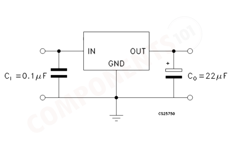
This circuit is capable of 5-volt output with up to 1A current. The L4941 voltage regulator maintains a constant output voltage regardless of changes in the input voltage or load conditions. The IN pin is where the unregulated input voltage is applied. The capacitor connected to the IN pin is labelled Ci and has a value of 0.1 μF. This capacitor helps to filter out any noise or voltage spikes from the power supply and provides a stable input voltage to the regulator. It also helps to reduce high-frequency noise and improve the transient response of the regulator.
The OUT pin is where the regulated output voltage is provided. The capacitor connected to the OUT pin is labelled Co and has a value of 22 μF. This capacitor helps to stabilize the output voltage by smoothing out any fluctuations and providing a steady voltage to the load. It also improves the transient response and ensures that the regulator can handle sudden changes in load current without significant voltage deviations. The GND pin of the regulator is connected to the ground of the circuit, providing a common reference point for the input and output voltages. The negative terminals of both capacitors (Ci and Co) are also connected to the ground.
Having Troubles with L4941?
The circuit’s performance is not stable, output voltage drops sometimes. Make sure the load is not drawing excessive current and the input source can provide enough current. Also, make sure the input and output filter capacitors are present and are with the recommended values.
How to add additional reverse polarity protection to the circuit?
To add reverse polarity protection to a circuit using the L4941, you can use a diode in series with the input supply. When the input supply is connected with the correct polarity, the diode conducts and allows the voltage to pass through to the L4941. If the input supply is connected with reverse polarity, the diode blocks the current, protecting the L4941 from damage.
Is a heat sink necessary for the working of L4941?
yes. For most applications, the L4941 needs a heat sink within its specified operating conditions.
What are the design considerations when designing a PCB using L4941?
Keep the output capacitor and input capacitors as close to the input and output pins as possible. Make a solid ground plane with limited vias.
Applications of L4941
- Battery-Powered Systems
- Power Supply for ECUs.
- Consumer Electronics
- Portable Devices
- Wearable Devices
- Industrial Applications
- Microcontroller Power Supply
- Battery Chargers
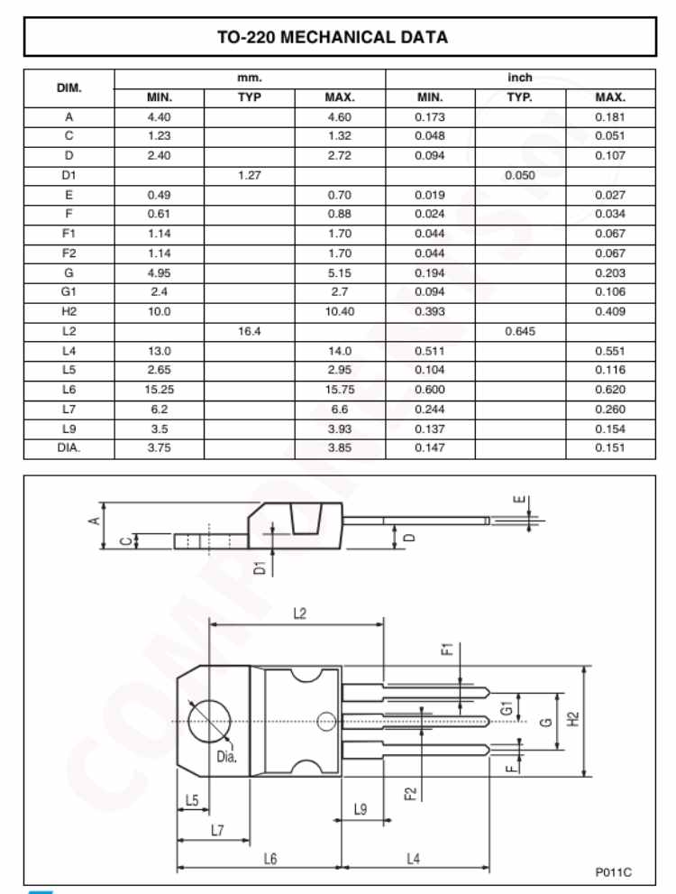
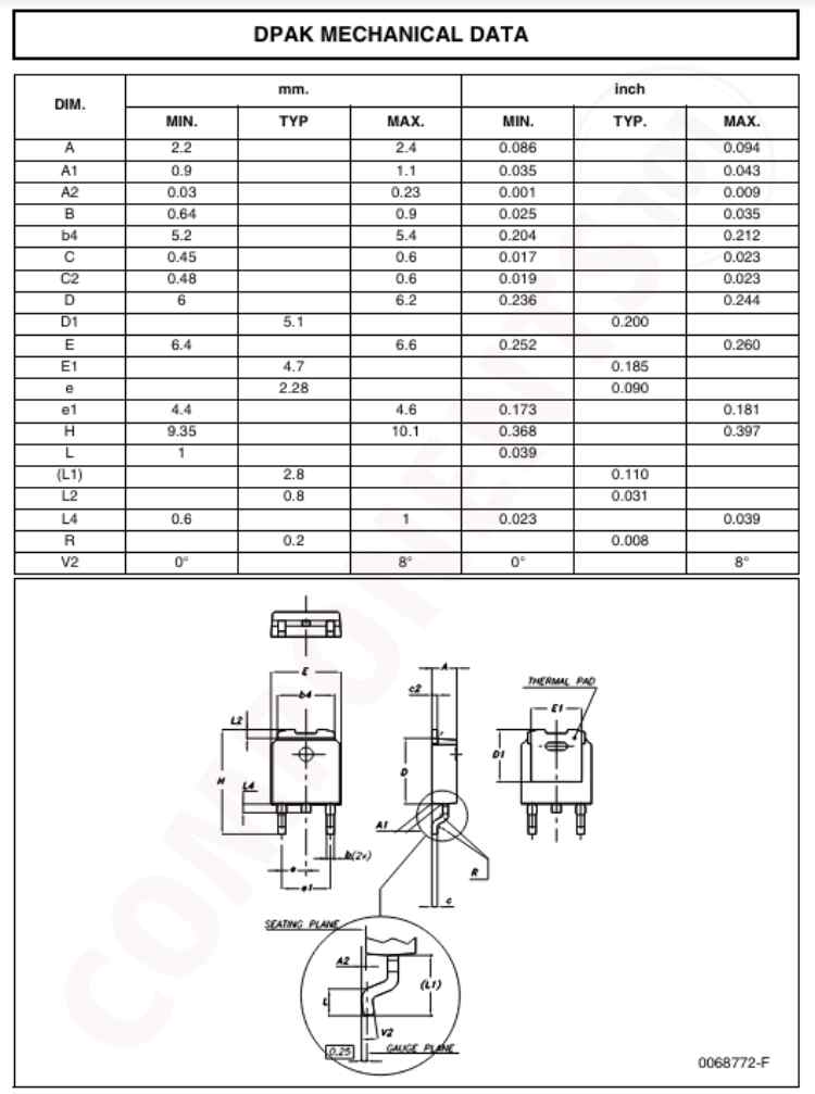
2D Model and Dimensions of L4941
Here you can find the mechanical drawings of LTC1734 along with its dimensions. The dimensions can be used to create custom footprints of the IC and be used for PCB or CAD modelling.