IRF4905 P-Channel MOSFET Pinout, Specifications, Equivalent & Datasheet
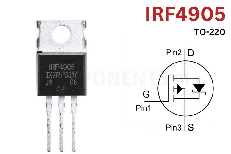
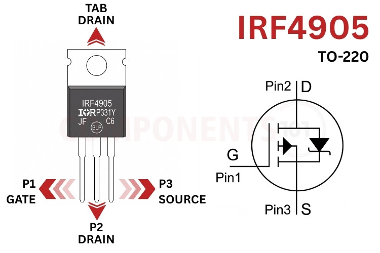
IRF4905 Pinout Configuration
The IRF4905 follows the standard JEDEC TO-220AB 3-pin configuration:
| Pin Number | Pin Name | Description |
| 1 | Gate (G) | Voltage control terminal. Pulling the Gate negative relative to the Source (VGS ≤ -4V to -10V) switches the MOSFET fully ON. |
| 2 | Drain (D) | High-current power terminal connected to the load. Internally bonded to the metallic TO-220 mounting tab. |
| 3 | Source (S) | Power terminal connected to the positive DC power supply rail in typical high-side switching topologies. |
| Tab | Drain (D) | Metallic mounting heatsink tab electrically connected to Pin 2 Drain for maximum thermal conduction. |
*Note: Because the metallic heatsink tab is bonded to Pin 2 Drain, mounting multiple MOSFETs on a shared metal chassis requires electrical insulation (mica/sil-pad with shoulder washers) to prevent short circuits between switched load channels.
IRF4905 Key Features & Specifications
- Transistor Polarity / Type: P-Channel Enhancement-Mode HEXFET Power MOSFET
- Drain-to-Source Breakdown Voltage (V(BR)DSS): -55V (at VGS = 0V, ID = -250 µA)
- Continuous Drain Current (ID): -74A at TC = 25°C; -52A at TC = 100°C (VGS = -10V)
- Pulsed Drain Current (IDM): -260A (pulse width limited by maximum junction temperature)
- Maximum Power Dissipation (PD): 200W at TC = 25°C (linear derating factor 1.3 W/°C above 25°C)
- Static Drain-to-Source On-Resistance (RDS(on)): 20 mΩ (0.02 Ω) max at VGS = -10V, ID = -38A
- Gate Threshold Voltage (VGS(th)): -2.0V min to -4.0V max at VDS = VGS, ID = -250 µA
- Gate-to-Source Voltage (VGS): ±20V max
- Forward Transconductance (gfs): 21 S min at VDS = -25V, ID = -38A
- Package Type: TO-220AB (Through-Hole 3-Lead Power Package)
*Note: Complete Technical Details can be found in the IRF4905 datasheet given at the end of this page.
IRF4905 Equivalent & Alternative Components
| Equivalent Part | Polarity | Key Ratings | Description & Compatibility Notes |
| IRF3205 | N-Channel | 55V, 110A, 8.0 mΩ, TO-220AB | Direct complementary N-channel partner for high-power H-bridge motor driver circuits. |
| IRF5305 | N-Channel | -55V, -31A, 60 mΩ, TO-220AB | Lower-current 31A sibling in the same -55V family; suitable for moderate 10A-15A DC loads. |
| FQP27P06 | P-Channel | -60V, -27A, 70 mΩ, TO-220 | Fairchild / onsemi alternative with a slightly higher breakdown margin (-60V). |
| NDP6020P | P-Channel | -20V, -24A, 50 mΩ, TO-220 | Logic-level threshold P-channel MOSFET for direct 3.3V/5V low-voltage battery disconnects. |
| SUP60020E | P-Channel | -60V, -120A, 4.3 mΩ, TO-220 | Modern ultra-low RDS(on) Vishay Siliconix upgrade for ultra-high-current automotive designs. |
| IRFB4110 | N-Channel | 100V, 180A, 4.5 mΩ, TO-220AB | High-power benchmark N-channel MOSFET for high-voltage (48V-72V) low-side switching. |
Brief Description of IRF4905
The IRF4905 is the benchmark power MOSFET for high-side switching in automotive and heavy industrial DC systems. Manufactured using International Rectifier's fifth-generation planar stripe cell architecture, it achieves an extraordinarily low on-resistance of 20 mΩ for a -55V rated P-channel device. Because hole mobility in silicon is naturally two to three times lower than electron mobility, P-channel MOSFET dies require significantly larger silicon area to match the conductance of an equivalent N-channel device. The IRF4905 achieves its 74A rating through this expanded active die area, giving it massive thermal mass, low thermal resistance (0.75 °C/W), and an exceptional single-pulse avalanche ruggedness rating of 930 mJ.
Key operational characteristics of the IRF4905 include:
1. High-Side Power Rail Interfacing: By tying the Source to +12V or +24V, the switched load remains permanently connected to ground (common chassis return). This prevents ground loop offsets, simplifies load current sensing, and satisfies stringent automotive electrical safety standards where grounded loads must remain unpowered when disconnected.
2. Gate Drive Voltage Requirements (VGS): The threshold voltage (VGS(th)) sits between -2.0V and -4.0V, but complete channel saturation with minimum RDS(on) (20 mΩ) requires pulling the Gate 10V below the Source (VGS = -10V). Driving the gate with only -5V results in higher channel resistance and severe thermal dissipation under heavy loads.
3. Gate-to-Source Overvoltage Protection (±20V Max): On a 12V system, grounding the gate creates VGS = -12V, which safely saturates the MOSFET. However, on 24V or 36V DC systems, grounding the gate would pull VGS to -24V or -36V, causing catastrophic dielectric breakdown of the thin silicon gate oxide. In higher-voltage circuits, a resistive divider or a 12V Zener clamping diode across Gate and Source is mandatory.
4. Heatsinking and Current Derating: While the silicon die is rated up to -74 A at TC = 25°C, sustained operation above 20A requires a substantial finned aluminum heatsink. At 40A of continuous load current, on-state conduction loss generates approximately P = I² x RDS(on) = (40A)² x 0.02 Ω = 32W of heat, necessitating thermal interface material with low contact resistance.
IRF4905 Datasheet
The complete original manufacturer electrical characteristics, safe operating area (SOA) curves, switching waveforms, and thermal impedance characteristics are available in the official Infineon PDF IRF4905 datasheet.
How to Use the IRF4905 in a Circuit
To interface the IRF4905 with the 3.3V or 5V GPIO output of a modern microcontroller (such as an Arduino, ESP32, or STM32), a small-signal transistor is deployed as an open-collector level shifter to translate logic signals to the 12V/24V high-side power domain.
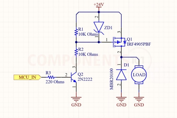
Circuit Operation & Component Selection
1. Pull-Up Resistor (R1 = 10 kΩ):
Connected directly between the IRF4905 Gate and Source (+VCC rail), resistor R1 holds the gate at +VCC whenever the control transistor is turned OFF. This ensures VGS = 0V, keeping the IRF4905 firmly in cutoff and preventing accidental conduction during microcontroller reboot or high-impedance reset states.
2. NPN Level-Shifter Transistor (Q2 = 2N2222A or BC547):
Because a 3.3V or 5V microcontroller pin cannot swing up to 12V or 24V, NPN transistor Q2 acts as an open-collector level shifter:
- When MCU GPIO is LOW (0V), Q2 is OFF. Resistor R1 pulls the IRF4905 Gate to +VCC (VGS = 0V), turning the MOSFET OFF.
- When the MCU GPIO is HIGH (3.3V / 5.0V), base resistor R3 (1 kΩ) saturates Q2, pulling current down through divider resistor R2 to ground. This sinks the IRF4905 Gate voltage below the Source rail, turning the MOSFET ON.
3. Voltage Divider & Zener Clamp Protection (R2 = 10 kΩ, ZD1 = 12V 1N4742A):
On 24V power systems, resistors R1 (10 kΩ) and R2 (10 kΩ) form a 50% voltage divider, dropping the gate to +12V relative to ground (VGS = -12V relative to Source), perfectly saturating the MOSFET while keeping VGS well within its ±20V absolute maximum rating. Zener diode ZD1 (12V) connected across Gate and Source clamps any high-voltage inductive transients or alternator load dumps below 12V, providing robust overvoltage immunity.
4. Inductive Flyback Clamping Diode (MBR20100 / 1N5408):
When driving high-current inductive loads (such as DC motors, winches, heavy contactors, or solenoids), sudden turn-off induces an inductive back-EMF voltage spike of opposite polarity. A fast-recovery Schottky diode (such as a 20A MBR20100) connected across the load terminals clamps this kickback safely to ground, shielding the IRF4905 Drain from exceeding its -55V breakdown threshold.
Applications
- Automotive High-Side Power Switching: Headlight controllers, high-power cooling fan modulators, horn drivers, and 12V/24V accessory power gating.
- DC Motor H-Bridges & Directional Drives: High-side power switches in bidirectional H-bridges paired with low-side IRF3205 N-channel MOSFETs.
- Reverse Battery Polarity Protection: Ultra-low on-resistance power gating replacing lossy high-current diodes in off-grid solar and automotive electronics.
- Battery Management Systems (BMS) & Solar Charge Controllers: High-side battery disconnect and load shedding switches in 12V, 24V, and 36V lithium/lead-acid systems.
- Heavy-Duty Relay & Solenoid Actuation: Spark-free solid-state switching for industrial contactors, hydraulic solenoid valves, and winch relays.
- Power Distribution Units (PDUs): High-current load ganging and overcurrent protection switches in telecommunications and server power supplies.
2D Model and Component Dimensions
For PCB layout engineers and CAD designers drafting footprint libraries in KiCad, Altium Designer, Eagle, or EasyEDA, the mechanical dimensions for the standard TO-220AB (PG-TO220-3-U05) package are detailed below (conforming to Infineon / International Rectifier packaging standards):
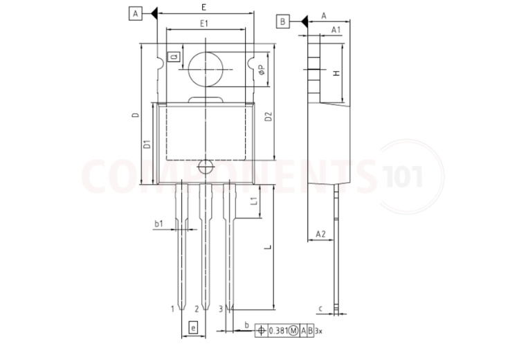
| Parameter Symbol & Description | Minimum (mm) | Typical (mm) | Maximum (mm) |
| A (Total Package Thickness / Depth) | 3.56 | - | 4.83 |
| A1 (Mounting Tab Thickness) | 1.14 | - | 1.40 |
| A2 (Lead Offset / Base to Seating Plane) | 2.03 | - | 2.92 |
| b (Lead Width, X3) | 0.38 | - | 1.01 |
| b1 (Lead Shoulder Width, X3) | 1.14 | - | 1.78 |
| c (Lead Thickness) | 0.36 | - | 0.61 |
| D (Total Body Length / Height) | 14.22 | - | 16.51 |
| D1 (Molded Plastic Body Height) | 8.38 | - | 9.20 |
| D2 (Tab Notch Reference Height) | 11.68 | - | 12.88 |
| E (Total Molded Body Width) | 9.65 | - | 10.67 |
| E1 (Mounting Tab Width) | 6.86 | - | 8.89 |
| e (Lead Pitch / Pin Spacing) | - | 2.54 | - |
| H (Upper Exposed Heatsink Tab Height) | 5.84 | - | 6.86 |
| L (Lead Length Below Seating Plane) | 12.70 | - | 14.73 |
| L1 (Lead Shoulder Length) | 3.56 | - | 4.06 |
| ØP (Mounting Hole Diameter) | 3.54 | - | 4.08 |
| Q (Tab Top to Mounting Hole Center) | 2.54 | - | 3.42 |