PIC18F4550 Microcontroller
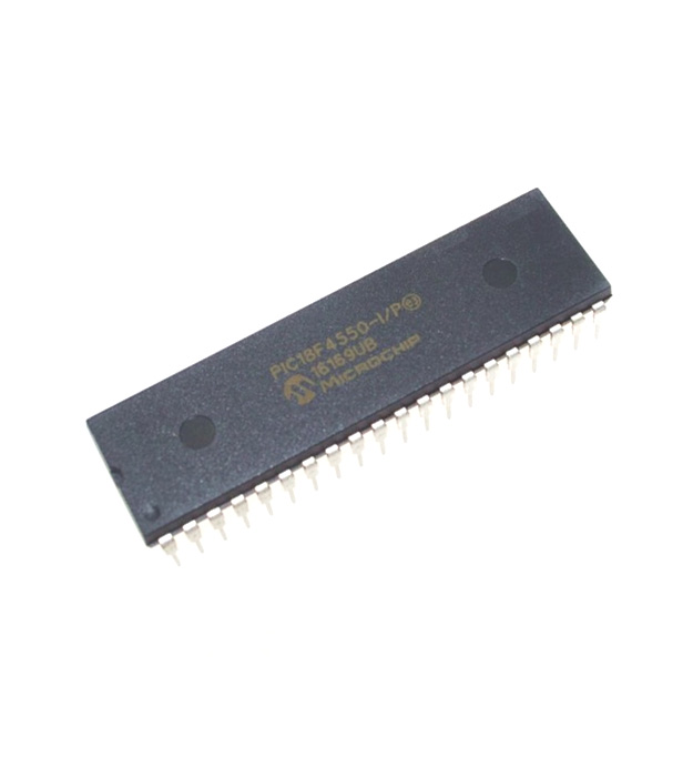
PIC18F4550 belongs to ‘PIC18F’ family of microcontrollers. PIC18F4550 is one of popular Microcontrollers from the microchip technology, comes with a High-Performance, Enhanced flash, USB Microcontroller with nano-Watt-Technology. This is an 8-bit microcontroller popular among makers and engineers due its features and easy applications. PIC18F4550 comes in various packages like DIP, QPF and QPN and can be selected according to the project requirement.
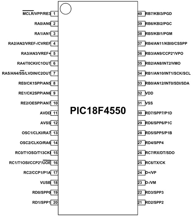
PIC18F4550 Pinout Configuration
It is a 40 pin device as shown in PIC18F4550 pin diagram. There are so many features for a controller the manufacturer cannot provide that many I/O pins. So many pins of controller have multiple features. These features can be enabled through programming depending on requirement. We will describe each pin functions briefly below.
|
Pin Number |
Pin Name |
Description |
|
1 |
MCLR/VPP/RE3 |
MCLR: Master Clear(RESET) Input VPP:programming voltage input RE3: I/O pin of PORTE, PIN 3 |
|
2 |
RA0/AN0 |
RA0: I/O pin of PORTA, PIN 0 AN0: Analog input 0 |
|
3 |
RA1/AN1 |
RA1: I/O pin of PORTA, PIN 1 AN1: Analog input 1 |
|
4 |
RA2/AN2/VREF-/CVREF |
RA2: I/O pin of PORTA, PIN 2 AN2: Analog input 2 VREF-: A/D reference voltage (low) input CVREF: Analog comparator reference output |
|
5 |
RA3/AN3/VREF+ |
RA3: I/O pin of PORTA, PIN 3 AN3: Analog input3 VREF+: A/D reference voltage (high) input |
|
6 |
RA4/T0CKI/C1OUT/RCV |
RA4: I/O pin of PORTA, PIN 4 T0CKI: Timer0 external clock input C1OUT: Comparator 1 output RCV:External USB transceiver RCV input |
|
7 |
RA5/AN4/SS/HLVDIN/C2OUT |
RA5: I/O pin of PORTA, PIN 5 AN4: Analog input 4 SS: SPI slave select input HLDVIN: High/Low-Voltage Detect input C2OUT: Comparator 2 output |
|
8 |
RE0/AN5/CK1SPP |
RE0: I/O pin of PORTE, PIN 0 AN5: Analog input 5 CK1SPP: SPP clock 1 output |
|
9 |
RE1/AN6/CK2SPP |
RE1: I/O pin of PORTE, PIN 1 AN6: Analog input 6 CK2SPP: SPP clock 2 output |
|
10 |
RE2/AN7/OESPP |
RE2: I/O pin of PORTE, PIN 2 AN6: Analog input 7 OESPP : SPP Enabled output |
|
11 |
VDD |
Positive Power Supply (+5V) |
|
12 |
VSS |
Ground |
|
13 |
OSC1/CLKI |
OSC1:Oscillator pin 1 CLKI: External clock source input |
|
14 |
OSC2/CLKO/RA6 |
OSC2: Oscillator pin 2 CLKO: clock source output RA6: I/O pin of PORTA, PIN 6 |
|
15 |
RC0/T1OSO/T13CKI |
RC0: I/O pin of PORTC, PIN 0 T1OSO :Timer1 oscillator output T13CKI: Timer1/Timer3 external clock input |
|
16 |
RC1/T1OSI/CCP2/UOE |
RC1: I/O pin of PORTC, PIN 1 T1OSI: Timer1 oscillator input CCP2:Capture 2 input/Compare 2 output/PWM2 output UOE: External USB transceiver OE output |
|
17 |
RC2/CCP1/P1A |
RC2: I/O pin of PORTC, PIN 2 CCP1: Capture 1 input/Compare 1 output/PWM1 output. P1A :Enhanced CCP1 PWM output, channel A |
|
18 |
VUSB |
VUSB:Internal USB 3.3V voltage regulator output |
|
19 |
RD0/SPP0 |
RD0: I/O pin of PORTD, PIN 0 SPP0: Streaming Parallel Port data |
|
20 |
RD1/SPP1 |
RD1: I/O pin of PORTD, PIN 1 SPP1: Streaming Parallel Port data |
|
21 |
RD2/SPP2 |
RD2: I/O pin of PORTD, PIN 2 SPP2: Streaming Parallel Port data |
|
22 |
RD3/SPP3 |
RD3: I/O pin of PORTD, PIN 3 SPP3: Streaming Parallel Port data |
|
23 |
RC4/D-/VM |
RC4: I/O pin of PORTC, PIN 4 D-: USB differential minus line (input/output) VM: External USB transceiver VM input |
|
24 |
RC5/D+/VP |
RC5: I/O pin of PORTC, PIN 5 D+: USB differential plus line (input/output). VP: External USB transceiver VP input |
|
25 |
RC6/TX/CK |
RC6: I/O pin of PORTC, PIN 6 TX: EUSART asynchronous transmit CK: EUSART synchronous clock (see RX/DT). |
|
26 |
RC7/RX/DT/SDO |
RC7: I/O pin of PORTC, PIN 7 RX: EUSART asynchronous receive DT: EUSART synchronous data (see TX/CK). SDO: SPI data out |
|
27 |
RD4/SPP4 |
RD4: I/O pin of PORTD, PIN 4 SPP4: Streaming Parallel Port data |
|
28 |
RD5/SPP5/P1B |
RD5: I/O pin of PORTD, PIN 5 SPP5: Streaming Parallel Port data P1B: Enhanced CCP1 PWM output, channel B |
|
29 |
RD6/SPP6/P1C |
RD6: I/O pin of PORTD, PIN 6 SPP6: Streaming Parallel Port data P1C: Enhanced CCP1 PWM output, channel C |
|
30 |
RD7/SPP7/P1D |
RD7: I/O pin of PORTD, PIN 7 SPP7: Streaming Parallel Port data P1D: Enhanced CCP1 PWM output, channel D |
|
31 |
VSS |
Ground |
|
32 |
VDD |
Positive Power Supply (+5V) |
|
33 |
RB0/AN12/INT0/FLT0/SDI/SDA |
RB0: I/O pin of PORTB, PIN 0 AN12: Analog input 12 INT0: External interrupt 0 FLT0: Enhanced PWM Fault input (ECCP1 module) SDI: SPI data in SDA: I2C data I/O |
|
34 |
RB1/AN10/INT1/SCK/SCL |
RB1: I/O pin of PORTB, PIN 1 AN10: Analog input 10 INT1: External interrupt 1 SCK: Synchronous serial clock input/output for SPI mode SCL: Synchronous serial clock input/output for I2C mode |
|
35 |
RB2/AN8/INT2/VMO |
RB2: I/O pin of PORTB, PIN 2 AN8: Analog input 8 INT2: External interrupt 2 VMO: External USB transceiver VMO output |
|
36 |
RB3/AN9/CCP2/VPO |
RB3: I/O pin of PORTB, PIN 3 AN9: Analog input 9 CCP2: Capture 2 input/Compare 2 output/PWM2 output VPO: External USB transceiver VPO output |
|
37 |
RB4/AN11/KBI0/CSSPP |
RB4: I/O pin of PORTB, PIN 4 AN11: Analog input 11 KBI0: Interrupt-on-change pin CSSPP: SPP chip select control output |
|
38 |
RB5/KBI1/PGM |
RB5: I/O pin of PORTB, PIN 5 KBI1: Interrupt-on-change pin PGM: Low-Voltage ICSP Programming enable pin |
|
39 |
RB6/KBI2/PGC |
RB6: I/O pin of PORTB, PIN 6 KBI2: Interrupt-on-change pin PGC: In-Circuit Debugger and ICSP programming clock pin. |
|
40 |
RB7/KBI3/PGD |
RB7: I/O pin of PORTB, PIN 7 KBI3: Interrupt-on-change pin PGD: In-Circuit Debugger and ICSP programming data pin. |
Features
|
PIC18F4550 – Simplified Features |
|
|
CPU |
8-bit |
|
Total Number of Pins |
40 |
|
Operating Voltage |
+4.0 to +5.5 V (+5.5V being absolute maximum) |
|
Number of programmable I/O pins |
35 |
|
Communication Interface |
USB Serial Interface (23,24 PINS) [Can be used for programming this controller] Master/Slave SPI Serial Interface(7,26,33, 34 PINS) [Can be used for programming this controller] Programmable Serial UART(25,26 PINS) [Can be used for programming this controller] Two-wire Serial Interface(33, 34 PINS)[Can be used to connect peripheral devices like sensors and LCDs] |
|
ADC Module |
13channels, 10-bit resolution ADC |
|
Timer Module |
One 8-bit counter, Three 16-bit counter |
|
Analog Comparators |
2 |
|
PWM channels |
4 |
|
External Oscillator |
Up to 48MHz |
|
Internal Oscillator |
32KHz-8MHz Calibrated Internal Oscillator |
|
Program Memory Type |
Flash |
|
Program Memory |
32Kbytes[10000 write/erase cycles] |
|
CPU Speed |
12 MIPS |
|
RAM Bytes |
2KBytes |
|
EEPROM |
256Bytes |
|
Watchdog Timer |
Programmable Watchdog Timer with Separate On-chip Oscillator |
|
Power Save Modes |
Available |
|
Operating Temperature |
-40°C to +85°C(+85 being absolute maximum, -40 being absolute minimum) |
Note: More technical details can be found in the PIC18F4550 Datasheet, linked at the bottom of this page.
PIC18F4550 Replacements
PIC18F4455
PIC18F4550 Family
PIC18F2455, PIC18F2550
Where to use PIC18F4550 Microcontroller
PIC18F4550 is easy to program PIC controller. The controller program memory satisfies most applications. Along with 35 programmable Input/output pins, it can interface many peripherals easily. With Watchdog timer to reset under error it can be used on systems with no human interference. Having USB interface feature you can communicate with controller from any PC without any hassle. With many features added together further promotes use of PIC18F4550 controller.
How to Use PIC18F4550 Microcontroller
PIC18F4550 is used as any other microcontroller. Micro controllers are not like digital ICs. For working of PIC18F4550, first we need to save the appropriate program file in the controller FLASH memory. Once power is provided, the controller executes this code saved in FLASH memory to create the response.
Entire process of using PIC18F4550 goes like this -
- List the functions to be executed by PIC18F4550
- Write the functions in IDE application using relative programming language
- (MPLAB IDE for Windows OS [ www.microchip.com/mplabx-ide-windows-installer ]
- (For these IDE the functions should be written in ‘C’ language)
- After writing the desired program compile for error elimination using IDE.
- After successful compilation IDE application generates HEX file for the written program.
- Choose the programming device (usually ‘PIC kit 3’) which establishes communication between PC and PIC18F4550.
- Run the HEX file dumping software which is related to the chosen programming device.
- Choose the appropriate program HEX file.
- Burn the HEX file of program in PIC18F4550 flash memory using this program.
- Disconnect the programmer, connect the appropriate peripherals for the controller and power the system.
- After connecting the power the controller executes this HEX code saved in the memory and performers tasks as instructed.
Applications
There are thousands of applications for PIC18F4550 -
- Hobbyist and Engineer general projects
- Development board for learners
- Temperature control systems
- Analog signal measuring and manipulations.
- Embedded systems like coffee machine, vending machine.
- Motor control systems
- Peripheral Interface system
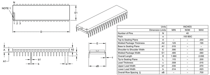
2D Model and Dimensions