ATmega128L 8-bit Atmel Microcontroller with 128KBytes In-System Programmable Flash
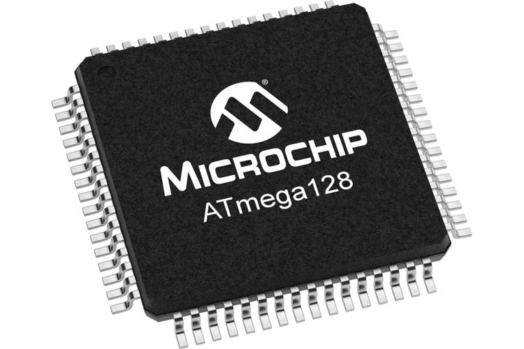
ATMEGA128L is a high-performance, low-power, 8-bit microcontroller from Microchip which is based on AVR RISC architecture. This microcontroller is not that popular among hobbyists and developers but if you are looking for medium power and reasonable price microcontroller from the Microchip AVR series, then this could be a great choice for you.
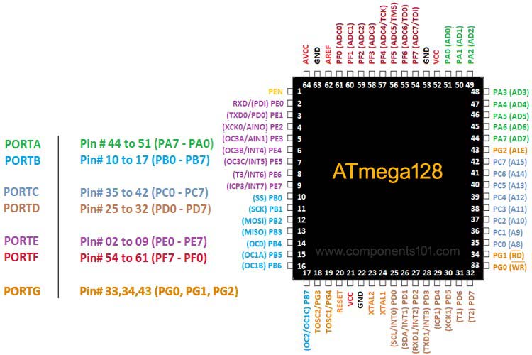
Atmega128L Pin Configuration
ATMEGA328P is a 64 pins chip as shown in the pin diagram above. Many pins of the chip here have more than one function. We will describe the functions of each pin in the below table.
|
Pin No |
Pin Name |
Pin Functions |
Description and Secondary Functions |
|
1 |
|
|
programming enable pin for the Serial Programming mode |
|
2 |
PE0 |
RXD0/(PDI) |
PDI/RXD0 (Programming Data Input or UART0 Receive Pin) |
|
3 |
PE1 |
TXD0/PDO |
PDO/TXD0 (Programming Data Output) or UART0 Transmit Pin |
|
4 |
PE2 |
XCK0/AIN0 |
Analog Comparator Positive Input or USART0 external clock input/output |
|
5 |
PE3 |
OC3A/AIN1 |
Analog Comparator Negative Input or Output Compare and PWM Output A for Timer/Counter3 |
|
6 |
PE4 |
OC3B/INT4 |
External Interrupt4 Input or Output Compare and PWM Output B for Timer/Counter3 |
|
7 |
PE5 |
OC3C/INT5 |
External Interrupt 5 Input or Output Compare and PWM Output C for Timer/Counter3 |
|
8 |
PE6 |
T3/INT6 |
External Interrupt 6 Input or Timer/Counter3 Clock Input |
|
9 |
PE7 |
ICP3/INT7 |
External Interrupt 7 Input or Timer/Counter3 Input Capture Pin |
|
10 |
PB0 |
|
SPI Slave Select input |
|
11 |
PB1 |
SCK |
SPI Bus Serial Clock |
|
12 |
PB2 |
MOSI |
SPI Bus Master Output/Slave Input |
|
13 |
PB3 |
MISO |
SPI Bus Master Input/Slave Output |
|
14 |
PB4 |
OC0 |
Output Compare and PWM Output for Timer/Counter0 |
|
15 |
PB5 |
OC1A |
Output Compare and PWM Output A for Timer/Counter1 |
|
16 |
PB6 |
OC1B |
Output Compare and PWM Output B for Timer/Counter1 |
|
17 |
PB7 |
OC2/OC1C |
Output Compare and PWM Output for Timer/Counter2 or Output Compare and PWM Output C for Timer/Counter1 |
|
18 |
PG3 |
TOSC2 |
RTC Oscillator Timer/Counter0 |
|
19 |
PG4 |
TOSC1/PG4 |
RTC Oscillator Timer/Counter0 |
|
20 |
|
|
|
|
21 |
VCC |
VCC |
Digital supply voltage |
|
22 |
GND |
GND |
Ground |
|
23 |
XTAL2 |
XTAL2 |
XTAL2 (Chip Clock Oscillator pin 2) |
|
24 |
XTAL1 |
XTAL1 |
XTAL1 (Chip Clock Oscillator pin 2) |
|
25 |
PD0 |
SCL/I NT0 |
External Interrupt0 Input or TWI Serial CLock) |
|
26 |
PD1 |
SDA/I NT1 |
External Interrupt1 Input or TWI Serial Data |
|
27 |
PD2 |
RXD1/I NT2 |
External Interrupt2 Input or UART1 Receive Pin |
|
28 |
PD3 |
TXD1/I NT3 |
External Interrupt3 Input or UART1 Transmit Pin |
|
29 |
PD4 |
ICP1 |
Timer/Counter1 Input Capture Pin |
|
30 |
PD5 |
XCK1 |
USART1 External Clock Input/Output |
|
31 |
PD6 |
T1 |
Timer/Counter1 Clock Input |
|
32 |
PD7 |
T2 |
Timer/Counter2 Clock Input |
|
33 |
PG0 |
|
Write strobe to external memory |
|
34 |
PG1 |
|
Read strobe to external memory |
|
35 |
PC0 |
A8 |
Compatibility mode can be used for External Memory Interface |
|
36 |
PC1 |
A9 |
Compatibility mode can be used for External Memory Interface |
|
37 |
PC2 |
A10 |
Compatibility mode can be used for External Memory Interface |
|
38 |
PC3 |
A11 |
Compatibility mode can be used for External Memory Interface |
|
39 |
PC4 |
A12 |
Compatibility mode can be used for External Memory Interface |
|
40 |
PC5 |
A13 |
Compatibility mode can be used for External Memory Interface |
|
41 |
PC6 |
A14 |
Compatibility mode can be used for External Memory Interface |
|
42 |
PC7 |
A15 |
Compatibility mode can be used for External Memory Interface |
|
43 |
PG2 |
ALE |
ALE is the external data memory Address Latch Enable signal. |
|
44 |
PA7 |
AD7 |
External memory interface address and data bit 7 |
|
45 |
PA6 |
AD6 |
External memory interface address and data bit 6 |
|
46 |
PA5 |
AD5 |
External memory interface address and data bit 5 |
|
47 |
PA4 |
AD4 |
External memory interface address and data bit 4 |
|
48 |
PA3 |
AD3 |
External memory interface address and data bit 3 |
|
49 |
PA2 |
AD2 |
External memory interface address and data bit 2 |
|
50 |
PA1 |
AD1 |
External memory interface address and data bit 1 |
|
51 |
PA0 |
AD0 |
External memory interface address and data bit 0 |
|
52 |
VCC |
VCC |
Digital supply voltage |
|
53 |
GND |
GND |
Ground |
|
54 |
PF7 |
ADC7/TDI |
ADC input channel 7 or JTAG Test Data Input |
|
55 |
PF6 |
ADC6/TDO |
ADC input channel 6 or JTAG Test Data Output |
|
56 |
PF5 |
ADC5/TMS |
ADC input channel 5 or JTAG Test Mode Select |
|
57 |
PF4 |
ADC4/TCK |
ADC input channel 4 or JTAG Test ClocK |
|
58 |
PF3 |
ADC3 |
ADC input channel 3 |
|
59 |
PF2 |
ADC2 |
ADC input channel 2 |
|
60 |
PF1 |
ADC1 |
ADC input channel 1 |
|
61 |
PF0 |
ADC0 |
ADC input channel 0 |
|
62 |
AREF |
AREF |
AREF is the analog reference pin for the A/D Converter |
|
63 |
GND |
GND |
Ground |
|
64 |
AVCC |
AVCC |
AVCC is the supply voltage pin for Port F and the A/D Converter. it should be connected to VCC through a low-pass filter. |
Note: Check the ATmega128L Datasheet attached at the bottom of the page for more information on compatibility mode.
Features & Specifications of ATmega128L
- Operating Voltage: 2.7 - 5.5V ATmega128L
- Frequency Grade: 0 - 8MHz ATmega128L
- High Endurance Non-volatile Memory segments
- 128Kbytes of In-System Self-programmable Flash program memory
- 4Kbytes EEPROM
- 4Kbytes Internal SRAM
- Write/Erase cycles: 10,000 Flash/100,000 EEPROM
- Two 8-bit PWM Channels
- 6 PWM Channels with Programmable Resolution from 2 to 16 Bits
- 8-channel, 10-bit ADC
- Master/Slave SPI Serial Interface
- Two Expanded 16-bit Timer/Counters with Separate Prescaler, Compare Mode, and Capture Mode
- Programmable Watchdog Timer with On-chip Oscillator
- On-chip Analog Comparator
- Two 8-bit Timer/Counters with Separate Prescaler
- Dual Programmable Serial USARTs
- Internal Calibrated RC Oscillator
- Software Selectable Clock Frequency
- JTAG (IEEE std. 1149.1 Compliant) Interface with Boundary Scan, on-chip debugging
- Optional Boot Code Section with Independent Lock Bits
- In-System Programming by On-chip Boot Program
- Data retention: 20 years at 85°C/100 years at 25°C
Similar Microcontrollers alike ATmega128L
ATmega8, ATmega88, ATmega8L, ATmega328L
How to Use ATMEGA128L
ATmega128L is a microcontroller that needs to be programmed otherwise it will do nothing like every other microcontroller out there. Without a program, this IC will do nothing but consume current to run internal functions. There are various ways to program an ATmega128L microcontroller, the most popular way is to use a USBasp Programmer with AVRDude as a programming interface, you can build and compile your program in order to get a HEX file. When you get your HEX file you can dump the HEX on this IC with the help of the AVRDUDE Program. Another way to program this device is to use the Arduino as ISP Programmer, if you have an Arduino in hand you can search the web for numerous examples of how to do so. The next option is for those who do not have an Arduino or an USBasp Programmer, this process is called is Parallel Programming, you have to use the Parallel Port which is only available in older Desktop PCs, if you do not have the port, you can always purchase a PCI Parallel port converter for cheap.
Where to Use ATMEGA128L
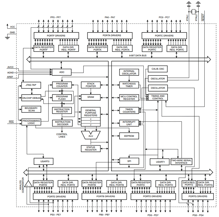
As we have said earlier the Atmega128L is not that popular in comparison to Arduino, although there is an old version of Arduino that uses the ATmega128L as its main Controller. As the price of this controller is less than the ATmega328P along with a program memory of 32 Kbytes. This microcontroller can be used in many battery-powered applications with a watchdog timer to reset under error. It can be used on systems with minimal human interference and also has an advanced multi-mode PWM output that can be used for many different applications. The block diagram of the ATmega128L is shown below-
Applications
There are hundreds of applications for ATMEGA328P:
- Industrial control systems.
- SMPS and Power Regulation systems.
- Digital data processing.
- Analog signal measuring and manipulations.
- Embedded systems like coffee machines, vending machines.
- Motor control systems.
- Display units.
- Peripheral Interface system.
2D Model and Dimensions
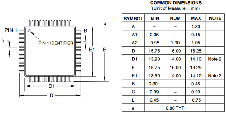
Below is the 2D model of the IC along with its dimensions in inches(millimeters). The following information can be used to design the custom footprints and be used for PCB designing and CAD modeling.
