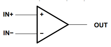
TL074 Op-Amp (JFET Input)
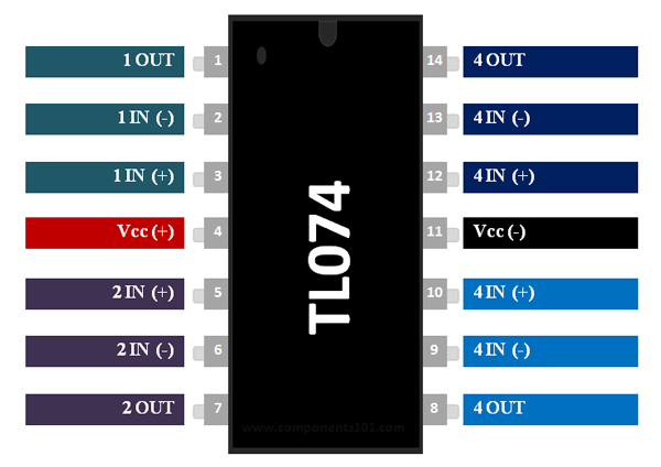
TL074 Pin Configuration
|
Pin Number |
Pin Name |
Description |
|
1,7,10,16 |
Op-Amp Output Pins |
These are the output pins of the four Op-Amps |
|
2,6,11,15 |
Input Inverting Pins |
These are the input inverting pins of the four Op-Amps |
|
3,5,12,14 |
Input Non-Inverting Pins |
These are the input non-inverting pins of the four Op-Amps |
|
4 |
Vcc (+) |
Positive Supply Rail of the Op-Amp |
|
13 |
Vcc (-) |
Negative Supply Rail of the Op-Amp |
Features and Specifications
- JFET Input Op-Amp Quad Package
- Typical Operating Voltage: +15V to -15V
- Maximum operating Voltage: 36V
- Input Bias Current: 65pA
- Common mode Rejection Ratio CMRR: 100dB
- Low Level Input Voltage: 0.8V (max)
- Propagation Delay (Pd) / Transition time: 29 ns (max)
- Low Input Bias and Offset Current
- Output Short circuit protection
- Available in 14-pin PDIP, SO-14, TSSOP packages with variations like TL74A, TL74AB, TL74AC, and TL74L.
Note: Complete Technical Details can be found in the TL074 IC datasheet given at the end of this page.
TL074 Equivalent
Alternatives Op-Amps
LM741A, LM741C, LM709C, LM201, MC1439, and LM748
Where to use TL074 IC
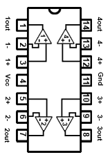
The TL074 is a Quad Package Operational Amplifier, meaning it has four Op-Amps inside it and each Op-Amp can be used independently.
The main distinguishing feature of the TL074 Op-Amp is that they incorporate high-voltage JFET and bipolar transistors which helps the transistor to have very high input impedance and low bias current. Also this Op-Amp has low noise and harmonic distortion making it an ideal choice for audio pre-amplifiers. So if you are looking for an Op-Amp IC with Quad package and JFET driven then this IC might be the right choice for you
How to use TL074 Op-Amp
TL074 is very similar to the LM324 Op-Amp, they both have four Op-Amps inside them and have the exact same pinouts. However they differ a bit in their characteristics since the TL074 has a JFET inside it. If you are curious to learn about few application circuits of this IC then you can read through how LM324 is used since both the IC shares the same applications.
TL074 Op-Amp Design Considerations
The Op-Amps as we know are the work horse for most electronics circuit designs. There are a plethora of application circuits for Op-Amp each having its characteristics and significance in its own way. But every Op-Amp designs will have some common design considerations or tips which are common among them and we will discuss the same further.
Inputs: Op-Amps are known for its high input impedance, meaning it will not draw any current (or disturb) the signal that is being given to the Input pin. The input stage of an Op-Amp is mostly complex since it involves many stages. The Input common-mode range value must be considered while supplying voltage signals because the input voltage should never exceed the rail voltage else it will create a latch-up condition which in return will create a short circuit of the supply voltage and thus damaging the circuit permanently. Also the difference between the voltage values of the Inverting and the Non-Inverting pin should not be more than the Differential Input Voltage Rating.
Output: The TL074 is not a rail to rail Op-Amp hence the output voltage will not reach the maximum positive or maximum negative voltage when saturated. It will always be ~2V less than the supply voltage, this voltage drop occurs because of the Vce voltage drop of the transistors present inside the Op-Amp. Also remember that a saturated Op-Amp will comparatively draw more current and thus results in power loss.
Gain/Feedback: Op-Amps are known for their very large Open-Loop Gain, but sadly this gain is accompanied by noise hence most of the circuits are designed using Closed-Loop. A Closed-Loop system provides feedback to the input this limiting the gain value of the Op-Amp and the noise associated with it. A Negative feedback is commonly preferred, since it has predictable behaviour and stable operation.
Terminating Unused Op-Amp pins
For ICs like TL074 that has a Quad Op-Amp style package, often there is a good chance that the design does not utilize all the available four Op-Amps. In those case it is very important to terminate the Unused Op-Amp properly. Else, the unused pins will develop some stay capacitance which might pick up noise and affect the performance, also non terminated Op-Amps will consume more power thus decreasing the efficiency of the design. There are many ways to terminate an Op-Amp based on your design, but the most common used method is shown below.
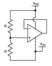
Here the Op-Amp is operating between the voltage range Vdd and Vss. To terminate the Op-Amp the Inverting pin of the Op-Amp is connected to the Output pin and the Non-Inverting pin is provided with a constant voltage source. This constant voltage could be of any value but must be within the limits of supply voltage (Common mode Voltage Range). Hence it is not mandatory to have these two resistors since any available voltage of that particular range from the circuit can be used to terminate the Non-Inverting pin of the Op-Amp.
Applications
- Circuit requiring high input impedance
- Buffer application
- Filter circuits, Voltage followers
- Integrator, Differentiator, Summer, adder, Voltage follower, etc.,
- DC gain blocks
- Comparators (Loop control & regulation)
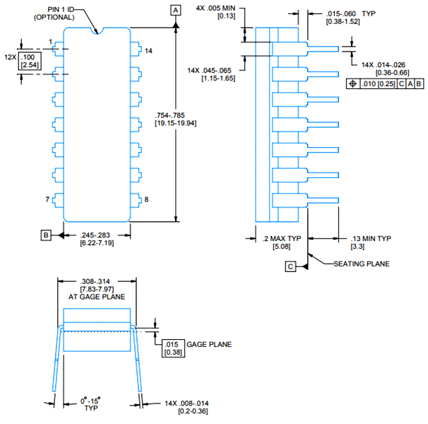
2D Model (CDIP)