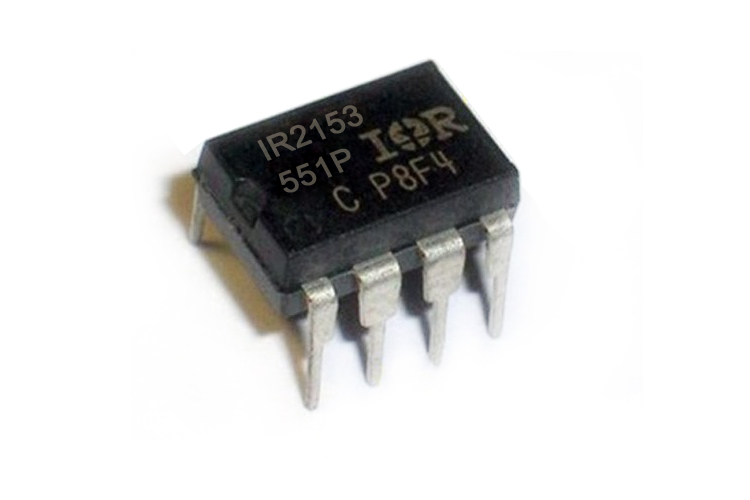
IR2153 Self-Oscillating Half-Bridge MOSFET Driver
The IR2153D is an improved version of the popular IR2155 and IR2151 gate driver ICs, and incorporates a high voltage half-bridge gate driver with a front-end oscillator similar to the industry standard CMOS 555 timer.
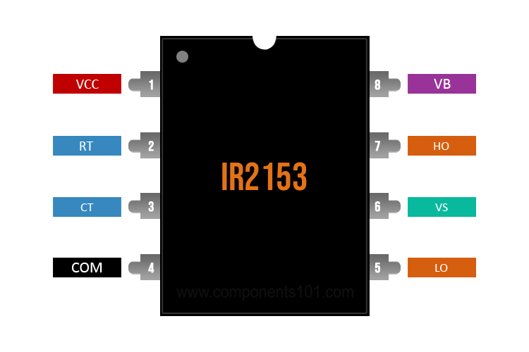
IR2153D Pinout Configuration
|
Pin Number |
Pin Name |
Description |
|
1 |
VCC |
Logic and internal gate drive supply voltage |
|
2 |
RT |
Oscillator timing resistor input |
|
3 |
CT |
Oscillator timing capacitor input |
|
4 |
COM |
IC power and signal ground |
|
5 |
LO |
Low side gate driver output |
|
6 |
VS |
High voltage floating supply return |
|
7 |
HO |
High side gate driver output |
|
8 |
VB |
High side gate driver floating supply |
Features & Specifications
- Integrated 600V half-bridge gate driver
- 15.6V Zener clamp on Vcc
- True micropower start up
- Tighter initial deadtime control
- Low temperature coefficient deadtime
- Shutdown feature (1/6th Vcc) on CT pin
- Increased undervoltage lockout Hysteresis (1V)
- Lower power level-shifting circuit
- Constant LO, HO pulse widths at start-up
- Lower di/dt gate driver for better noise immunity
- Low side output in phase with RT
- Internal 50nsec (typ.) bootstrap diode (IR2153D)
- Excellent latch immunity on all inputs and outputs
- ESD protection on all leads
- Also available LEAD-FREE
Note: Complete Technical Details can be found in the IR2153 datasheet given at the end of this page.
IR2153 Equivalent ICs
IR44272, IR44273, IR44252, IR2100, IR2122
Where to use IR2153 MOSFET Gate Driver
The IR2153 is an improved version of the popular IR2155 and IR2151 gate driver ICs. The IR2153 provides more functionality and is easier to use than previous ICs. A shutdown feature has been designed into the CT pin, so that both gate driver outputs can be disabled using a low voltage control signal. In addition, the gate driver output pulse widths are the same once the rising undervoltage lockout threshold on VCC has been reached, resulting in a more stable profile of frequency vs time at start-up. Noise immunity has been improved significantly, both by lowering the peak di/dt of the gate drivers, and by increasing the undervoltage lockout hysteresis to 1V. Finally, special attention has been paid to maximizing the latch immunity of the device, and providing comprehensive ESD protection on all pins.
As this IC is a half-bridge gate driver IC that can be used in many different applications like DC-DC power supplies, Inverters, motor driver, solenoid river, high side MOSFET drivers can be used for protection relay power distribution and motor driver applications.
Basic Features and Maximum Rating of IR2153 IC
This IC has some interesting features that one must know in order to work with this IC. The high side floating supply voltage is 25V maximum, the high side floating supply offset voltage is 3V, the RT and CT pin is VCC + 0.3 Volts respectively, and the applied current for this IC is 25mA. The slew rate for this IC is 50V/nS. The maximum power dissipation for this IC is 1W. Maximum junction temperature is 150 °C.
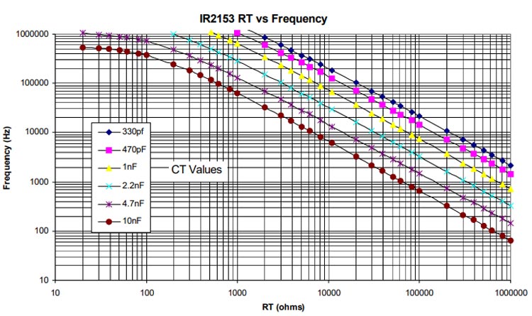
The above figure shows you the frequency response when using different RT and CT values, in this device
How to use IR2153 MOSFET Gate Driver
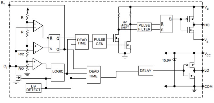
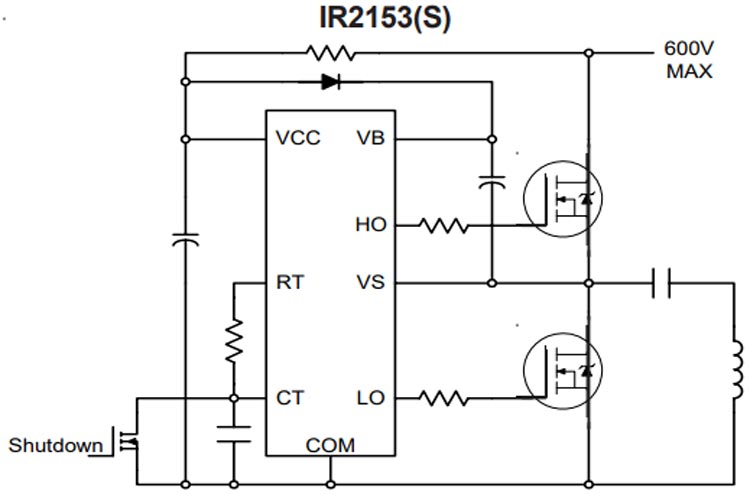
As the name suggest this IC is mostly used to drive the gate of the MOSFET. A MOSFET gate driver is required when there is a need to switch a MOSFET with extreme efficiency. The image below shows a basic schematic of the configuration of the IR2153
Applications
- Industrial controls
- Automatic Test Equipment (ATE)
- HVAC controls
- Medical devices
- Internet of Things
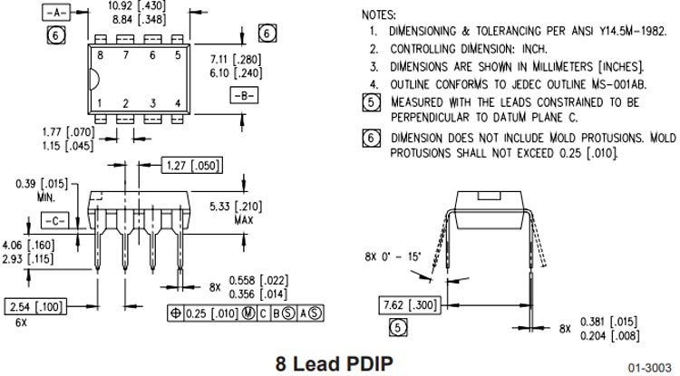
2D Model and Dimensions
If you are designing a PCB or Perf board with this component then the following picture from the Datasheet will be useful to know its package type and dimensions.