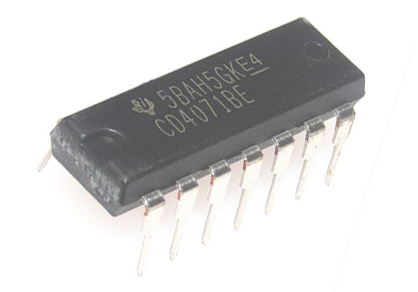
CD4071 - Dual-Input OR Gate IC
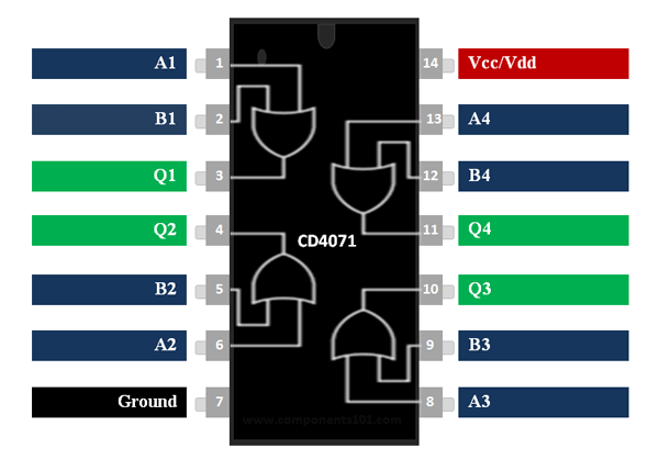
CD4071 Pin Configuration
|
Pin Number |
Pin Name |
Description |
|
1,6,10,15 |
OR Gate Input pin (A) |
First Input pin for the OR gate |
|
2,5,11,14 |
OR Gate Input pin (B) |
Second Input pin for the OR gate |
|
3,4,12,13 |
OR Gate Output pin (Q) |
Output pin for the OR gate |
|
7 |
Ground |
Connect to the ground of the circuit. |
|
14 |
Vcc (Vdd) |
Used to power the IC. Typically +5V is used |
Features
- Dual Input OR Gate – Quad Package
- Typical Operating Voltage: 5V
- Operating Voltage Range: -0.5V to +20V
- DC input current: ±10mA
- Power Dissipation: 500mW
- Minimum logic Low voltage @+5V: 1.5V
- Minimum Logic High voltage @+5V: 3.5V
- Propagation Delay @5V : 250ns (maximum)
- Transition Time @5V :200ns (maximum)
- Available in 14-pin PDIP, GDIP, PDSO packages
Note: Complete Technical Details can be found in the CD4071 datasheet provided below this article.
CD4071 Equivalent
Other Logic Gates
74LS00, 74LS08, 74LS02, 74LS04, 74HCT04
Where to use CD4071 IC
The CD4071 is a Dual Input OR Gate with Quad package. Meaning it has four OR gate IC inside it, each of which can be utilized independently. AND gates are used in building Logic level circuits like Encoder, Decoder multiplexers etc. Logic level gates like CD4071 and flip-flops play a vital role in digital electronics.
If you are looking for an IC to perform logic level OR operation with two inputs, then this IC might be the right choice for you. If you have more than two inputs for your OR gate, then you should look into three input and four input OR gates.
Logic OR explanation
The logic OR operation is very simple, since this is a two input OR gate we will have only two inputs which is A and B respectively. The output of the OR gate is called as Q. The truth table for the OR gate is shown below.
|
A |
B |
Q |
|
0 |
0 |
0 |
|
1 |
0 |
1 |
|
0 |
1 |
1 |
|
1 |
1 |
1 |
How to use CD4071 IC
TO use the CD4071 IC, just power it using the Vcc (pin 14) and ground (pin 8) lines. The typical operating voltage of the IC is +5V, but it can also be operated in +5V, +10V and +15V. The output voltage of the IC on the pin Q will be equal to the operating voltage of the IC. As per the truth table shown above, when either one or both the input of the Gate is high the output will be high. The complete working of the gate with a sample CD4071 circuit is shown in the GIF file below.
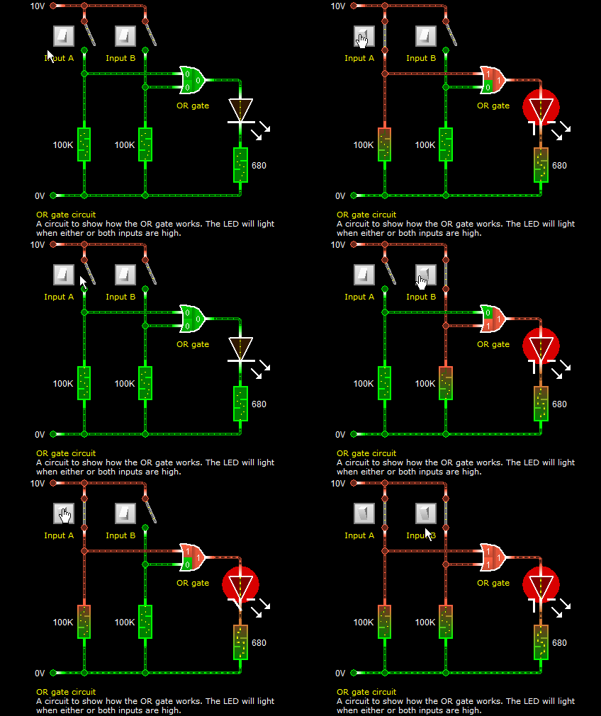
The input for the gate is controlled by using a switch connected to pin A and B of the Gate. A pull down resistor of 100k is used to hold the logic to low (logic 0) when the switch is left floating. To visualize the output we have connected a LED to the output pin Q. The resistor 680R is used to limit the current through the LED.
Applications
- Basic Logic Circuits
- Encoders and Decoders
- Multiplexers and De-multiplexers
- Oscillator circuits
- Networking and Digital Systems
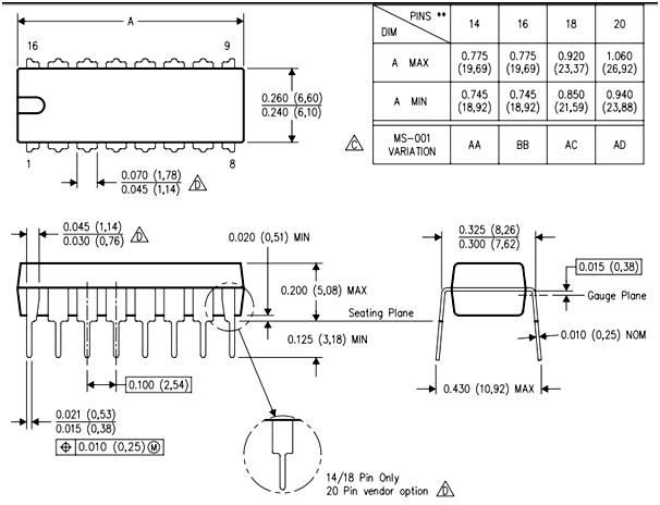
2D-Model and Dimensions
