74LS08 – Quadruple Two Input AND Gate
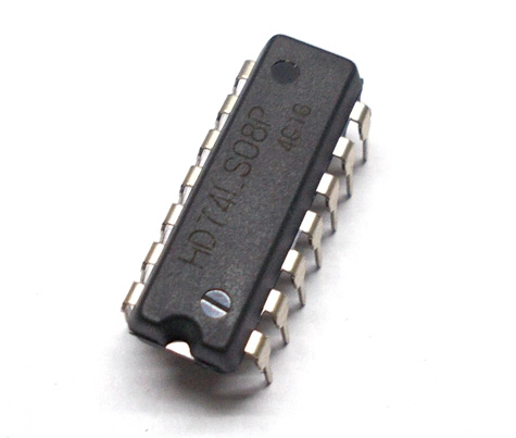
74LS08 IC is a member of 74XXYY IC series. There are four AND gates in the chip and each gate have two inputs, hence the name QUADRUPLE 2- INPUT AND GATE. The gates in the chip are designed by SCHOTTKY TRANSISTORS for high speed logic operations.
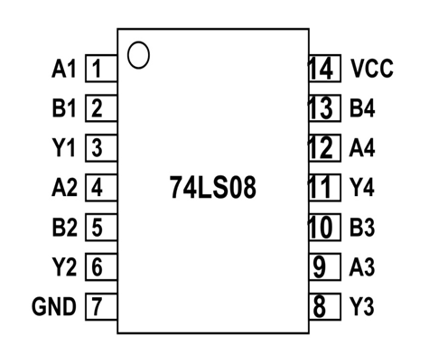
74LS08 Pin configuration
74LS08 is a 14 PIN IC. The chip is available in different packages and is chosen depending on requirement. The description for each pin is given below.
|
Pin Number |
Description |
|
AND GATE 1 |
|
|
1 |
A1-INPUT1 of GATE 1 |
|
2 |
B1-INPUT2 of GATE 1 |
|
3 |
Y1-OUTPUT of GATE1 |
|
AND GATE 2 |
|
|
4 |
A2-INPUT1 of GATE 2 |
|
5 |
B2-INPUT2 of GATE 2 |
|
6 |
Y2-OUTPUT of GATE2 |
|
AND GATE 3 |
|
|
9 |
A3-INPUT1 of GATE 3 |
|
10 |
B3-INPUT2 of GATE 3 |
|
8 |
Y3-OUTPUT of GATE3 |
|
AND GATE 4 |
|
|
12 |
A4-INPUT1 of GATE 4 |
|
13 |
B4-INPUT2 of GATE 4 |
|
11 |
Y4-OUTPUT of GATE4 |
|
SHARED TERMINALS |
|
|
7 |
GND- Connected to ground |
|
14 |
VCC-Connected to positive voltage to provide power to all four gates |
Features and Specifications
- Operating voltage range: +4.75 to +5.25V
- Recommended operating voltage: +5V
- Maximum supply voltage:7V
- Maximum current allowed to draw through each gate output: 8mA
- TTL outputs
- Low power consumption
- Typical Rise Time: 18ns
- Typical Fall Time: 18ns
- Operating temperature:0°C to 70°C
- Storage Temperature: -65°C to 150°C
Note: Complete technical details can be found in the 74LS08 Datasheet linked at the bottom of this page.
74LS08 Equivalents
SN54LS08, IC 7408, HEF4081, Any two transistors can be reconfigured to form a AND gate.
Where to Use 74LS08 IC
There are many applications of IC 74LS08. A few mentioned below.
1. The chip is basically used where AND logic operation is needed. There are four AND gates in the chip, we can use one or all gates simultaneously.
2. The chip is used in systems where high speed AND operation is needed. As mentioned earlier the gates in the chip are designed by SCHOTTKY TRANSISTORS to make the switching delays of gates less. Because of this the chip can be used for high speed AND operations.
3. 74LS08 is one of cheapest IC present in market for AND logic operation. It is really popular and is available everywhere.
4. The chip provides TTL outputs which are needed in some systems.
How to Use 74LS08 IC
The four AND gates in the chip mentioned earlier are connected internally as shown in diagram below.
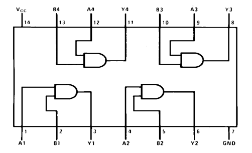
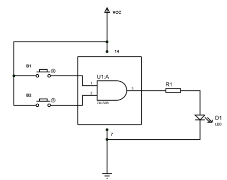
Each AND gate here performs AND operation for two logic inputs. For example gate1 performs AND operation between A1 and B1 and provides output at Y1 terminal.
The truth table of AND gate is given as,
|
Input1 |
Input2 |
AND Output |
|
LOW |
LOW |
LOW |
|
HIGH |
LOW |
LOW |
|
LOW |
HIGH |
LOW |
|
HIGH |
HIGH |
HIGH |
For realizing the above truth table let us take a simple AND gate application circuit as shown below.
For better understanding the internal working let us consider the simplified internal circuit of AND gate as shown below.
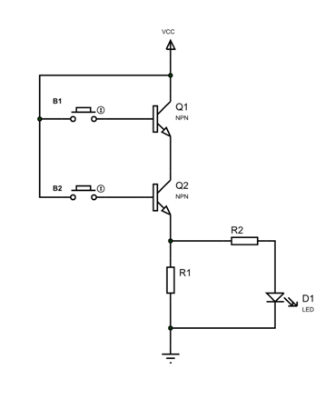
In the circuit two transistors are connected in series to form a AND gate. The two inputs of AND gate are driven out from bases of the two transistors. These two inputs are connected to buttons to change the logic of inputs. Output of the AND gate is the voltage across resistor R1. This output is connected to a LED D1 trough a current limiting resistor R2. This LED is connected to detect the state of output.
The circuit working can be explained in few stages below:
Stage1: When both buttons are not pressed. In this state the current flow through base of both transistors will be zero.Because base current is zeroboth transistors Q1 and Q2 will be OFF. So the total supply voltage VCC appears across the transistors Q1 and Q2. Because total VCC appears across transistors the drop across resistor R1 will be zero. Because output is nothing but voltage across resistor R1 it will be LOW. So when INPUTS = LOW, OUTPUT = LOW.
Stage2: When any one of the buttons is pressed.In this state the relative transistor will be ON leaving the other OFF. The ON transistor will act as short circuit and OFF transistor acts as open circuit having total VCC appearing across it. With that the drop across resistor R1 will be zero. Because output is nothing but voltage across resistor R1 it will be LOW. So when one INPUT = LOW, OUTPUT = LOW.
Stage3:When both buttons are pressed. Both transistors will be ON and voltage across both of them will be zero.At this time the total VCC appears across resistor R1.Because output is nothing but voltage across resistor R1 it will be HIGH. So when both INPUT = HIGH, OUTPUT = HIGH.
After verifying the three states, you can tell that we have satisfied the above truth table. We can also write the logic equation for AND gate by the truth table and is, Y = A.B or A+B
Like this we can use each gate of the chip depending on requirement.
Applications
- General purpose ANDlogic operation
- Measuring Instruments
- Digital Electronics
- Servers
- ALUs
- Memory units
- Networking
- Digital systems
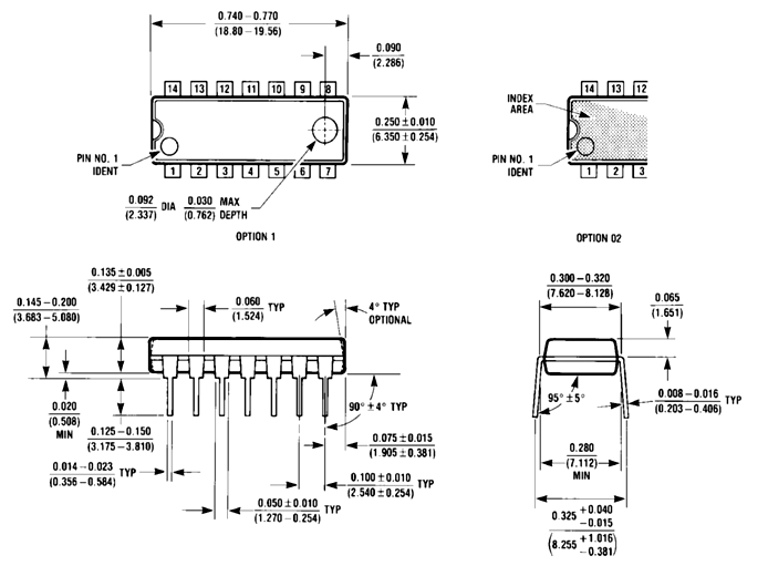
Dimensions
Measurements in (Inches/millimeters)