74HCT04 Hex Inverter IC
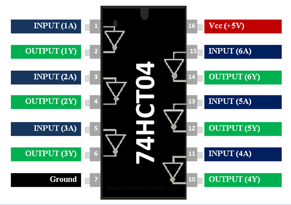
74HCT04 Pin Configuration
|
Pin Number |
Pin Name |
Description |
|
1,3,5,11,13,15 |
Input Pins |
Input pins of the NOT Gate (Inverter) |
|
2,4,6,10,12,14 |
Output Pins |
Output pins of the NOT Gate (Inverter) |
|
7 |
Ground |
Connected to the ground of the system |
|
16 |
Vcc (+5V) |
Powers the IC, typically with +5V |
Features
- Six Independent Inverter (NOT Gate) IC
- Operating Voltage: 4.5V to 5.5V
- Source/Sink Current: 4mA @4.5V (Vcc)
- Continuous Output Current: ±25mA
- High Level Input Voltage: 2V (min)
- Low Level Input Voltage: 0.8V (max)
- Propagation Delay (Pd) / Transition time: 29 ns (max)
- Input Pins have Schmitt trigger action
- All pins are TTL compatible
- Available in 14-pin PDIP, SO-14, TSSOP packages
Note: Complete Technical Details can be found at the 74HCT04 IC datasheet given at the end of this page.
74HCT04 Equivalents
74HC04
Alternatives Logic Gate IC
74HCT00, 74HCT02, 74HCT08, 74HCT32, 74HCT86
Where to use 74HCT04 Hex Inverter
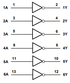
The 74HCT04 is a hex inverter IC, meaning it has 6 inverted (NOT Gates) inside it of which each NOT gate can perform independently on its own. NOT gates are very useful in building Logic Combinational Circuits; they can also work independently as a Wave oscillator or as a Buffer IC. Since the IC package has 6 Gates inside it, the connections get compact and the response of all 6 gates is almost identical making it more reliable.
So if you are looking for an IC which can help you Invert signals or if you circuit requires multiple NOT gates, then this IC might be the right choice for you.
How to Use 74HCT04 IC
As mentioned earlier 74LS14 has six INVERTING (NOT) GATES which can be used as six individual gates. It is very easy to use this IC since the pins are TTL compatible no much external components are required. Simply power the IC and provide the input signal and we will get the output on the corresponding pin. A working GIF is shown below.
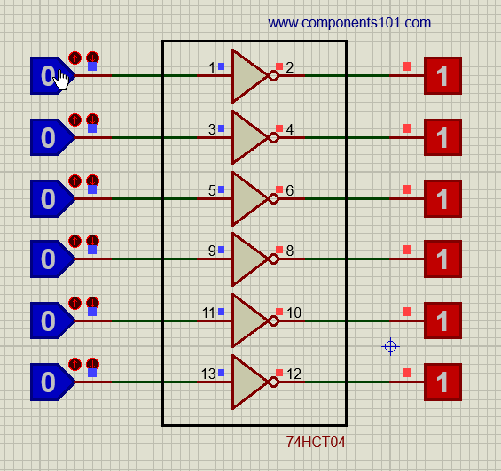
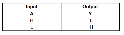
As you can see each of the 6 Gates can operate individually based on the input signal. It is also important to remember that in the above simulation the Power pin (pin 14) and ground pin (pin 7) is not shown, so in real circuit the ground pin has to be grounded and the power pin has to be provided with +5V. The truth table for a NOT gate is shown below, where A represents Input and Y represents output. If the Input is high the output will be low and of the input is low the output will be high, hence this IC got its name as inverter.
The maximum low level input voltage is 0.8V, anything more that that will be considered as high and the minimum high level voltage is 2V anything less that will be considered as low. So this IC can also operate with 3.31v signal lines making it suitable for a 3.3V to 5V logic level converter.
Propagation Delay of 74HCT04 IC
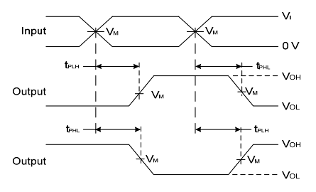
In gates like 74HCT04 switching time is an important parameter to consider when the IC acts as a wave oscillator or buffer. It is the ability of the IC on how quickly it toggle the output based on the change in input. The time taken for the output pin to change from one state to another state is called as propagation delay, which is around 29nS for this IC. A more detail switching diagram is shown below, the values of these parameters can be obtained from the 74HCT04 datasheet linked at the bottom of this page.
Applications
- Combinational Logic Circuits
- Buffer IC
- Wave oscillator
- Clock signal generators
- Square wave generators
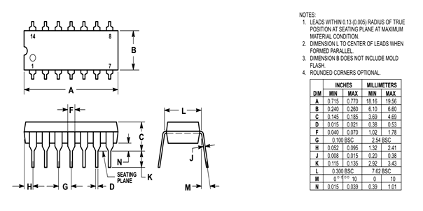
2D Model and Dimensions