CD4052 4-Channel Multiplexer/Demultiplexer IC

The CD4052 is a 4-Channel Multiplexer and Demulitplexer IC. It can either be used as a 4:1 Multiplexer or 1:4 Demultiplexer. The IC supports both Analog and Digital voltages and hence widely used in many designs.
Pin Configuration
|
Pin Number |
Pin Name |
Description |
|
16 |
Vdd |
Positive power input, maximum 20V |
|
7 |
Vee |
Negative power rail, normally connected to ground. |
|
8 |
Vss (Ground) |
Connected to ground of the circuit |
|
6 |
INH |
Enable pin – Must be pulled to ground for normal operation |
|
9,10 |
A,B |
Channel Select pins |
|
1,12 |
Y0,X0 |
Channel 0 Input / Output |
|
5,14 |
Y1,X1 |
Channel 1 Input / Output |
|
2,15 |
Y2,X2 |
Channel 2 Input / Output |
|
4,11 |
Y3,X3 |
Channel 3 Input / Output |
|
3,13 |
Y,X |
Common Output / Input |
Features
- 4-Channel Mux and Demux
- 4:1 Multiplexer IC
- 1:4 Demultiplexer IC
- Supports both Analog and Digital Voltage
- Nominal Voltage: 5V, 10V, 15V
- Maximum Operating Voltage: 20V
- Propagation Delay: 400ns at 5V
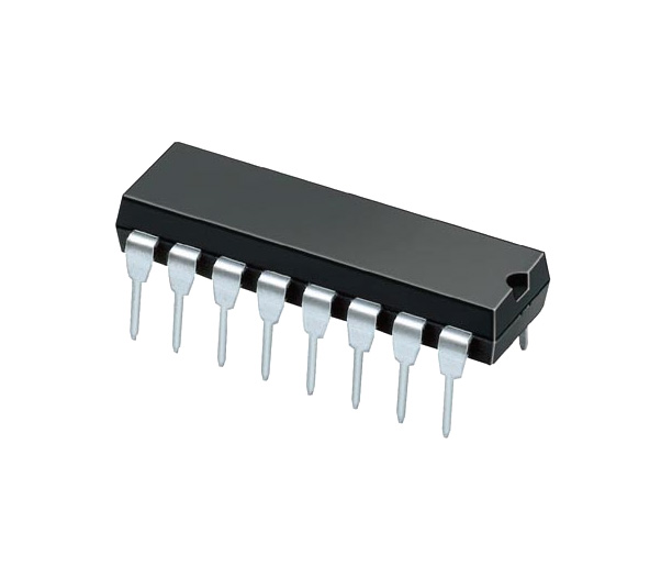
- Available in 16-pin PDIP, CDIP,SOIC, TSSOP packages
Note: Complete Technical Details can be found at the CD4052 datasheet given at the end of this page.
Alternatives Multiplexers
CD4052 Equivalents
NTE4052, 4017
Where to use CD4052 IC
The IC CD4052 is a CMOS based high voltage Multiplexer and Demultiplexer IC. The IC is commonly used in circuit where a 4:1 MUX or a 1:4 DEMUX is required in a Programmable Logic circuit Design. It can handle both analog and digital voltages hence can be used in Analog to Digital and Digital to Analog converters.
CD4052 as 4:1 Multiplexer:
The CD4052 can be used as a 4:1 Multiplexer, that is it can take inputs from 4-channel and convert it to single channel output based in the channel select pins. In our case the four Input channels are X0Y0, X1Y1, X2Y2 and X3 and Y3 and the single output channel is X,Y. The output on the single channel is decided based on the channel select pins A and B. The state of the select pins and channel selection is shown in below table:
|
A |
B |
Channel Selected |
|
0 |
0 |
Channel 0 |
|
1 |
0 |
Channel 1 |
|
0 |
1 |
Channel 2 |
|
1 |
1 |
Channel 3 |
The complete working of a 4:1 MUX using the CD4052 simulation is shown in the video below, the image here shows a snapshot of it.
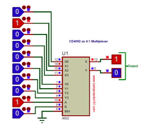
As you can see in the above image, the channel select pins are 1 and 0 for A and B respectively. Meaning the Channel 1 that is X1 and Y1 is selected. So the input given to X1 and Y1 is reflected on the pins X and Y.
CD4052 as 1:4 Demultiplexer:
The CD4052 can be used as a 1:4 Demultiplexer also, that is it can take one input and provide it either one of the 4 output channels based on the channel select pins. Here the input pins will be X and Y. The output pins can either be X0,Y0 or X1,Y1 or X2,Y2 or X3,Y3 based on the value set on A and B pins. We have already discussed the how to select the channel using pins A and B in the above table.
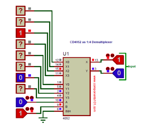
The above image shows the simulation of CD4052 in demultiplexer circuit, the complete working can be found in the video linked below. As you can see here, the channel 2 is selected by making A as 0 and B as 1. And hence the input given to pin X and Y is reflected on the channel 2 X2 and Y2 pins.
Applications
- Multiplexer and Demultiplxer circuit
- A/D and D/A converter circuits
- Network switching
- Programmable Logic circuits.
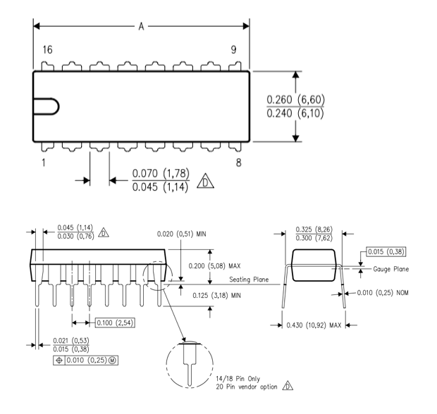
2D Model of CD4052 (PDIP):