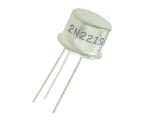
2N2219 NPN Transistor
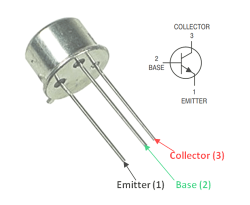
2N2219 Pin Configuration
|
Pin Number |
Pin Name |
Description |
|
1 |
Emitter |
Current Drains out through emitter, normally connected to ground |
|
2 |
Base |
Controls the biasing of transistor, Used to turn ON or OFF the transistor |
|
3 |
Collector |
Current flows in through collector, normally connected to load |
Features
- Small Signal NPN Transistor
- Current Gain (hFE), typically 50 for small signal
- Continuous Collector current (IC) is 800mA
- Collector-Emitter voltage (VCEO) is 50 V
- Collector-Base voltage (VCB0) is 75V
- Emitter Base Voltage (VBE0) is 6V
- Turn on time is 40ns
- Turn off time is 250ns
- Available in To-92 Package
Note: Complete Technical Details can be found in the 2N2219 datasheet given at the end of this page.
Alternative NPN Transistors
BC549, BC636, BC639, BC547, 2N2369, 2N3055, 2N3904, 2N3906, 2SC5200, 2N5551
2N2219 Equivalent Transistors
2N2905
Brief Description on 2N2219 Transistor
2N2219 is a NPN transistor hence the collector and emitter will be left open (Reverse biased) when the base pin is held at ground and will be closed (Forward biased) when a signal is provided to base pin. 2N2219 has a gain value hfe of 50; this value determines the amplification capacity of the transistor. The maximum amount of current that could flow through the Collector pin is 800mA, hence we cannot connect loads that consume more than 800mA using this transistor. To bias a transistor we have to supply current to base pin, this current (IB) should be limited to 5mA by using a transistor to the base pin.
When this transistor is fully biased then it can allow a maximum of 800mA to flow across the collector and emitter. This stage is called Saturation Region. When base current is removed the transistor becomes fully off, this stage is called as the Cut-off Region and the Base Emitter voltage could be around 600 mV.
Where to use 2N2219 Transistor
The 2N2219 transistor is very much similar to the commonly used NPN transistor 2N2222. But it comes in a metal can package and can operate on voltages slightly higher than what a 2N2222 can handle. Overall it is just another small signal transistor which is commonly used in switching and amplifying circuits.
So if you looking for an NPN transistor that could switch loads or for decent amplification then 2N2219 might the right choice for your project.
How to use 2N2219 as switch
The 2N2219 is a NPN transistor and is normally used as a switch in many circuits. So let’s discuss how to use one in a circuit. Since transistor is of NPN the load to be switched should be connected to the collector and the emitter should be connected to the ground as show in the figure below.
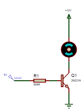
Another important thing to keep in mind, while using a transistor as switch is the base resistor. This resistor is connected to the base pin of the transistor to limit the current flowing through the base. As we know the transistor is a current controlled device meaning, we have pass some current (IB) thorough the base of the transistor to turn it on. The value of this current can be calculated by the required amount of current that will be consumed by the load. Here lets us assume the load here consumes around 800mA maximum so our collector current (IC) 800mA. To make this current flow through the transistor the value of base current IB can be calculated using the below formula:
IB = IC / hFE
Where hFE, is the current gain of the transistor which in our case is 50. In some cases the current gain will also be represented using the symbol β.
In our case for a collector current of 800mA we have to pass a base current of 16mA. So to calculate the resistor value of the base we can use the formulae
RB = (VCC – VBE) / IB
Where Vcc is the voltage on which the load operates and VBE is the voltage across the Base and Emitter which in our case according to the data sheet 1.3V. So the value if RB will be
RB = (12-1.3)/(16*10^-3)
= ~660 Ohms
However this vale will not be very accurate because the transistor will have an internal voltage drop across the collector current, so it mostly experimental to get the maximum current from the transistor. But this calculation will lead to the closest value to start with.
Applications
- Driver Modules like Relay Driver, LED driver etc..
- Amplifier modules like Audio amplifiers, signal Amplifier etc..
- Darlington pair
2D Model and Dimensions
If you are designing a PCB or Perf board with this component then the following picture from the 2N2219 Datasheet will be useful to know its package type and dimensions.
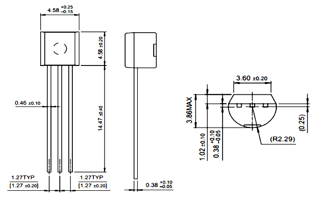


wrong 2D model linked…
wrong 2D model linked.
it's a TO-39/TO-5