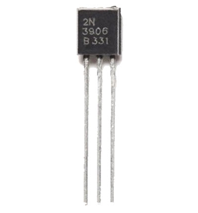
2N3906 PNP Transistor
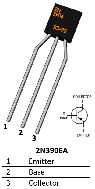
2N3906 Pin Configuration
|
Pin Number |
Pin Name |
Description |
|
1 |
Emitter |
Current Drains out through emitter |
|
2 |
Base |
Controls the biasing of transistor |
|
3 |
Collector |
Current flows in through collector |
Features
- Bi-Polar PNP Transistor
- DC Current Gain (hFE) is 300 maximum
- Continuous Collector current (IC) is 200mA
- Emitter Base Voltage (VBE) is 5V
- Base Current(IB) is 5mA maximum
- Collector Emitter Voltage (VCE) is 40V
- Collector Base Voltage (VCB) is 40V
- Available in To-92 Package
Note: Complete Technical Details can be found at the 2N3906 datasheet given at the end of this page.
2N3906 Equivalent Transistors
2N4403, MPSA13, MPSA92, MPSA55, ZTX555
Alternative for 2N3906
BC157, BC558, 2SA1943, BD140, S8550, TIP127, TIP42
Brief Description on 2N3906
2N3906 is a PNP transistor hence the collector and emitter will be closed (Forward biased) when the base pin is held at ground and will be opened (Reverse biased) when a signal is provided to base pin. This is where a PNP transistor differs from a NPN transistor, a Logic state (blue colour) is used to toggle between Ground and Signal Voltage (Emitter-Base Voltage VBE) as shown below
2N3906 has a gain value of 110 to 300, this value determines the amplification capacity of the transistor. The maximum amount of current that could flow through the Collector pin is 200mA, hence we cannot connect loads that consume more than 200mA using this transistor. To bias a transistor we have to supply current to base pin, this current (IB) should be limited to 5mA.
When this transistor is fully biased then it can allow a maximum of 200mA to flow across the collector and emitter. This stage is called Saturation Region and the typical voltage allowed across the Collector-Emitter (VCE) or Base-Emitter (VBE) could be 40 and 5 V respectively. When base current is removed the transistor becomes fully off, this stage is called as the Cut-off Region and the Base Emitter voltage could be around 5V.
Where to use 2N3906
The 2N3906 is a commonly used PNP transistor. It very much similar to the bc557 transistor except for that it has high collector to emitter voltage and hence high voltage loads can be toggled. This transistor has only a gain value of 300, hence not suitable for amplifier circuits.
So if you looking for a PNP transistor that could switch high voltage loads within 0.2A then this 2N3906 transistor might be the right choice for you.
How to use 2N3906
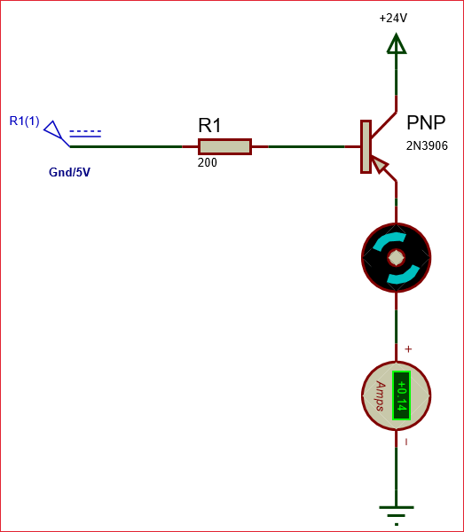
The 2N3906 transistor is commonly used as a switching device. When used as a switch, it can be operated in saturation region and cut-off region. In PNP transistor, by default it’s in ON state, but not to be said perfectly ON until the base pin is not grounded. If we provide ground to the base pin then the transistor will be in reverse biased and said to be turn ON. If supply is provided to the base pin it stops conducting current between emitter and collector and said to be in OFF state. For the protection of transistor a resistance added in series with it. For finding the value of that resistor you can use the formula:
RB = VBE / IB
Where, the value of VBE will be 5v for this transistor. The maximum value of providing base current is 200mA. So, from that you can find the value of resistance to be added in series with it. In the below circuit the base emitter voltage (VBE) is 0V (Grounded) hence the PNP transistor conducts and the motor rotates. If made high (5V) the motor will stop rotation. Note that for PNP transistors the loads should be connected in the collector side as shown below. Also note that the load current should be less than 200mA (here 140ma)
Applications
- Used to switch high voltage low current loads
- Optimal for loads with high peak voltage upto 40V
- It is used in the various switching applications.
- Used in inverter and converter circuits
- Used for making siren or dual Led or Lamp flasher.
- Can be used in Darlington Pair.
2D-Model and Dimensions
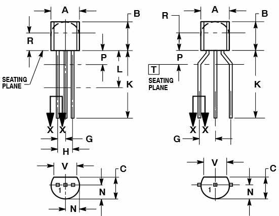
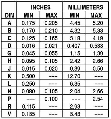
2D dimensions will help you in placing this component at the time of making circuit on perf board or a PCB.
