TC7660 Voltage Converter
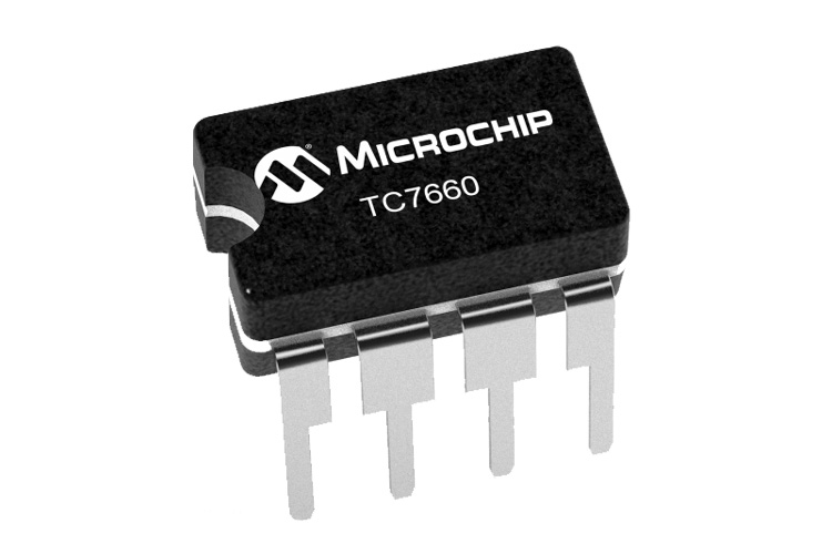
The TC7660 is a Charge Pump DC-to-DC Voltage Converter. It converts a +1.5V to +10V input to a corresponding -1.5V to -10V output using only two low-cost capacitors, eliminating inductors and their associated cost, size and electromagnetic interference (EMI).
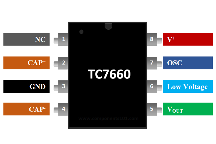
Pin Configuration of TC7660
|
Pin Number |
Pin Name |
Description |
|
1 |
NC |
No Connection |
|
2 |
CAP+ |
Charge pump capacitor positive terminal |
|
3 |
GND |
Ground Pin |
|
4 |
CAP- |
Charge pump capacitor negative terminal |
|
5 |
VOUT |
Output Voltage Pin |
|
6 |
Low Voltage |
Low Voltage Pin |
|
7 |
OSC |
Oscillator control input. Bypass with an external capacitor to slow the oscillator |
|
8 |
V+ |
Power Supply Pin |
Features & Specifications of TC7660
- Input Voltage Min: 1.5V
- Input Voltage Max: 10V
- Output Current: 20mA
- Adjustable Output Voltage Min: -10V
- Adjustable Output Voltage Max: -1.5V
- Low Power Consumption: 80 µA (typ) @ VIN = 5V
- Efficient Voltage Conversion (99.9%, typ)
- Available in 8-Pin Small Outline (SOIC), PDIP and CERDIP Packages
Note: Complete Technical Details can be found at the TC7660 datasheet given at the end of this page.
TC7660 Equivalent
ACT4514, CS51411, TS2580
Alternative DC-DC Controllers
MC34063A, LM2596, TC7660, MCP16252
Where to use TC7660 IC
The TC7660 is a Charge Pump DC-to-DC Voltage Converter IC and it is a pin-compatible replacement for the industry standard 7660 charge pump voltage converter. Since the regulation occurs through switching it is very efficient than linear circuits. The on-board oscillator operates at a nominal frequency of 10 kHz. Operation below 10 kHz (for lower supply current applications) is possible by connecting an external capacitor from OSC to ground.
The input voltage for the IC is from 1.5V to 10V and the output voltage can be varied from -1.5V to 10V and the maximum output current can be up to 20mA. So if you looking to design a DC-DC converter with the above specifications then TC7660 might be of interest to you.
How to use TC7660 IC
As mentioned above you only need two capacitors to use this IC. A Simple Negative Voltage
Converter circuit from TC7660 datasheet is shown below:
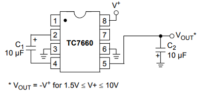
The TC7660 charge pump converter inverts the voltage applied to the V+ pin. Positive and Negative Pin of the charge pump capacitor (Pin 2 & 4), or flying capacitor, used to transfer charge from the input source to the output. In the voltage-inverting process, the charge pump capacitor is charged to the input voltage during the first half of the switching cycle and during the second half of the switching cycle, the charge pump capacitor is inverted and the charge is transferred to the output capacitor and load. For input voltages below 3.5V, the low voltage pin (Pin 6) should be connected to the ground. Otherwise, the low voltage pin should be allowed to float.
Applications of TC7660
- RS-232 Negative Power Supply
- Simple Conversion of +5V to ±5V Supplies
- Voltage Multiplication VOUT = ± n V+
- Negative Supplies for Data Acquisition Systems and Instrumentation
- Bluetooth Headsets
- +3.3V to +5.0V Distributed Power Supply
2D Model of TC7660
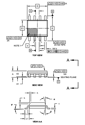
Dimensions for TC7660 IC are given below. These dimensions are for the SOIC package. If you are using different package IC please refer to the TC7660 datasheet.
