SN74LS166 8-Bit Shift Register
The SN74LS166AN is an 8-bit parallel-load serial-out Shift Register compatible with most other TTL logic families. This parallel-in or serial-in, serial-out shift register has a complexity of 77 equivalent gates on a monolithic chip. It features gated clock inputs and an overriding clear input. The parallel-in or serial-in modes are established by the shift/load input.
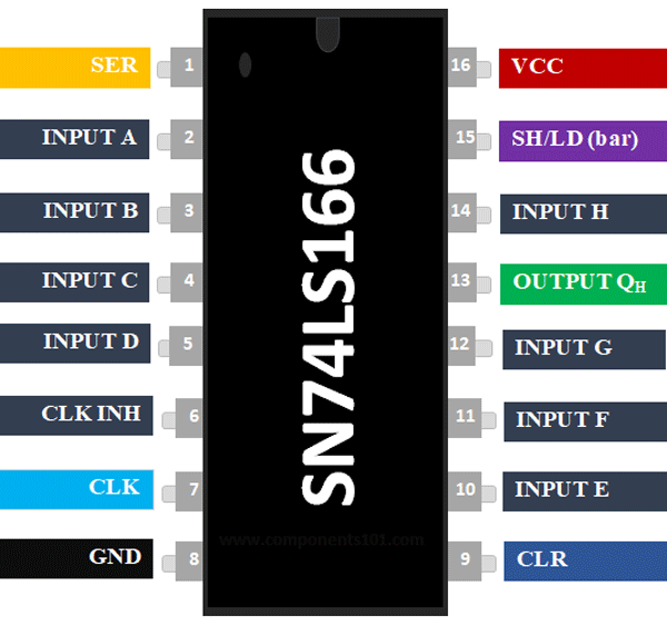
Pin Description of SN74LS166:
|
Pin Number |
Pin Name |
Description |
|
2, 3, 4, 5, 10, 11, 12, 14 |
A to H |
Parallel Data inputs. Data on these inputs are asynchronously entered in parallel into the internal flip–flops when the Serial Shift/Parallel Load input is low |
|
13 |
QH |
Complementary Shift Register output Pin |
|
1 |
SER |
Serial Input Pin. When the Serial Shift/Parallel Load input is high, data on this pin is serially entered into the first stage of the shift register |
|
6, 7 |
CLK INH & CLK |
Clock inputs. These two clock inputs function identically |
|
9 |
CLR |
Clear pin |
|
15 |
SH/LD |
Data–entry control input. |
|
8 |
VSS |
Ground |
|
16 |
VCC |
Supply Voltage – 5V, 10V, 15V |
Features of SN74LS166:
- 8-bit, Serial/Parallel to Serial Shift register
- Operating Voltage: 3V to 18V
- Supply Voltage - Max:5.25 V
- Propagation Delay Time: 25 ns
- Max. Clock Frequency: 35MHz
- Operating Temperature Range: 0C to + 70 C
- Available in 16-pin PDIP, GDIP, PDSO packages
Note: Complete Technical Details can be found at the SN74LS166 datasheet give at the end of this page.
Alternatives shift Registers:
|
Name |
Type |
|
74LS379 |
Quad Parallel Shift Register |
|
4014 |
4 Bit static shift register |
|
8 Bit Shift Register |
|
|
74LS323 |
8 Bit Shift/Storage Register |
|
74LS164 |
S/P Shift Register |
|
Dual 4 Bit Static Register |
|
|
74LS299 |
8 Bit Shift/Storage Register |
Where to use SN74LS166 IC
The SN74LS166 has an 8-bit parallel in or serial-in, serial-out Shift Register. Meaning it can receive (input) get data serially or parallel and control output pins in Serial. This comes in very handy where one does not have enough GPIO pins on our MCU/MPU to control the required number of outputs. It is often used in projects where relatively a large number of LEDs have to be controlled through the Microcontroller. It can also be used to interface the LCD screen since it can act as the data bit for the LCD displays.
How to use SN74LS166
The SN74LS166 shift register is commonly used with microcontrollers or microprocessors to expand the GIPO functionalities. SN74LS166 needs 4 lines of a microcontroller. One for the Clock, one to the enable the clock, one for shifting the bits, and one for the serial data transfer. To use SN74LS166 with microcontroller connect these four pins (SER, CLK INH & CLK, and SH/LD) to GPIO pins of the microcontroller. Input pins (A to H) can be connected to some type of input like buttons, switches, etc.
Applications of SN74LS166:
- Counters, Registers
- Arithmetic-unit registers
- Shift-left -shift-right registers
- Serial-to-parallel/parallel-to-serial conversions
- Sequence generation
- Control circuits
- Code conversion
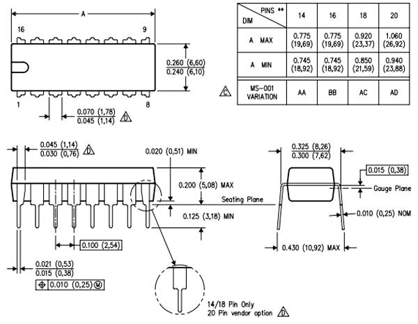
2D Model of SN74LS166 (PDIP):