74HC595 8-bit Shift Register
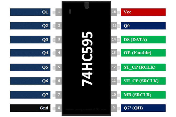
Pin Configuration
|
Pin Number |
Pin Name |
Description |
|
1,2,3,4,5,6,7 |
Output Pins (Q1 to Q7) |
The 74hc595 has 8 output pins out of which 7 are these pins. They can be controlled serially |
|
8 |
Ground |
Connected to the Ground of the circuit |
|
9 |
(Q7) Serial Output |
This pin is used to connect more than one 74hc595 as cascading |
|
10 |
(MR) Master Reset |
Resets all outputs as low. Must be held high for normal operation |
|
11 |
(SH_CP) Clock |
This is the clock pin to which the clock signal has to be provided from MCU/MPU |
|
12 |
(ST_CP) Latch |
The Latch pin is used to update the data to the output pins. It is active high |
|
13 |
(OE) Output Enable |
The Output Enable is used to turn off the outputs. Must be held low for normal operation |
|
14 |
(DS) Serial Data |
This is the pin to which data is sent, based on which the 8 outputs are controlled |
|
15 |
(Q0) Output |
The first output pin. |
|
16 |
Vcc |
This pin powers the IC, typically +5V is used. |
Features
- 8-bit, Serial In – Parallel out Shift register
- Operating Voltage: 2V to 6V
- Power Consumption: 80uA
- Output source/sink current: 35mA
- Output Voltage is equal to Operating voltage
- Minimum high-level Input Voltage: 3.15V @(Vcc=4.5V)
- Maximum low-level Input Voltage: 1.35V @(Vcc=4.5V)
- Can be easily cascaded with more IC to get more outputs
- Maximum Clock Frequency: 25Mhz @4.5V
- Available in 16-pin PDIP, GDIP, PDSO packages
Note: Complete technical details can be found in the 74HC595 datasheet given at the end of this page.
Alternatives Shift Registers
|
S.No: |
Name |
Type |
|
1 |
4035 |
4-Bit Parallel in Parallel out Shift Register |
|
2 |
74LS379 |
Quad Parallel Shift Register |
|
3 |
4014 |
4 Bit static shift register |
|
4 |
74LS166 |
8 Bit Shift Register |
|
5 |
74LS323 |
8 Bit Shift/Storage Register |
|
6 |
74LS164 |
S/P Shift Register |
|
7 |
4015 |
Dual 4 Bit Static Register |
|
8 |
74LS299 |
8 Bit Shift/Storage Register |
Where to Use 74HC595 IC
The 74HC595 is an 8-bit Serial In – Parallel Out Shift Register, i.e. it can receive (input) data serially and control 8 output pins in parallel. This comes in very handy where do not have enough GPIO pins on our MCU/MPU to control the required number of outputs. It is often used in projects where relatively a large number of LED’s has to be controlled through the Microcontroller. It can also be used to interface LCD screen since they can acts as the data bit for the LCD displays. It can also be used to control 5V loads like relays through a 3.3V microcontroller since the high-level voltage is only 3.15. So if you are looking for an IC to save on your GPIO pins on the Microcontroller, then this IC might be the right choice for you.
How to Use a 74HC595 IC
The 74HC595 shift register is commonly used with microcontrollers or microprocessors to expand the GIPO functionalities. It requires only 3 pins connected to the MCU, which are Clock, Data, and Latch. It has a wide operating voltage from 2V to 6V. An application circuit of the IC is shown below:
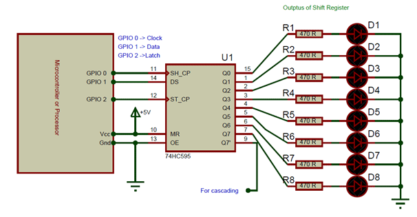
The pins 11, 14 and 12 are connected to the GPIO pins of the Microcontroller. In which pin 11 is the clock which sends a constant pulse to keep timing. The pin 14 is Data which actually sends the Data about which output pins has to stay low and which should go high. The Pin 12 is the Latch which updates the received the data to the output pins when made high, this pin can also be permanently held high. The below image will help you understand better.
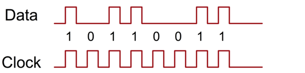
As you can see the clock is continues train of pulses, and the data goes high only at the respective place where the output has to get high. Here for example the binary value 0b10110011 is passed to the microcontroller. The pin Master reset (MR) is used to reset the outputs, when not in use it is held high to vcc, similarly the pin should be held low when not in use.
Another important advantage of the 74hc595 IC is that it can be cascaded to control more than 8 outputs. To do this, we use the Q7’ (pin 9), this pin should be connected to the data pin of the second 74HC595 IC. This way the first 8-bit sent from MCU will be used by the 1st IC and the second 8-bit will be used by the 2nd IC.
Applications
- Expand the GPIO pin on a MCU/MPU
- LED Matrix/Cube Projects
- Interface LCD
- Cascading applications
- High logic level controller
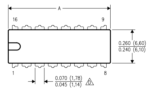
2D Model of 74HC595 (PDIP)