Infineon Launches OptiMOS™ 7 40 V MOSFETs to Improve Efficiency and Power Density in AI Server
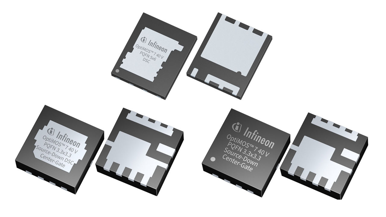
Infineon Technologies AG has launched its OptiMOS™ 7 40 V switching-optimised power MOSFET portfolio, designed to meet the demanding power-conversion requirements of AI servers, data centres, and telecommunications infrastructure. This portfolio is engineered for high-frequency DC-DC power conversion, aiming to significantly enhance efficiency and power density in space-constrained systems. The new devices are designed to address power conversion needs in both emerging 800 V DC architectures and established 48 V power architectures.
The OptiMOS™ 7 40 V devices are intended for the low-voltage secondary-side stages of high-voltage intermediate bus converters in 800 V DC architectures, as well as for intermediate bus converters in 48 V power architectures. Infineon states that the portfolio supports switching frequencies exceeding 1 MHz in suitable topologies, making these MOSFETs highly relevant for their target applications in AI server power conversion, data centers, and telecom infrastructure.
A core characteristic of the OptiMOS™ 7 40 V portfolio is its balanced approach to three crucial electrical parameters: on-state resistance (RDS(on)), output charge (Qoss), and gate charge (Qg). Infineon designed these devices to simultaneously tackle both conduction and switching losses. When compared to its OptiMOS 6 predecessor (IQE013N04LM6CGSC), the source-down device IQE010N04LM7CGSC demonstrates a reduction of up to 33 per cent in maximum RDS(on) at a gate-source voltage of 4.5 V. Furthermore, the figures of merit for both output charge and gate charge are reduced by up to 35 per cent in the same comparison.
Optimized for a 5 V gate drive, the portfolio also supports gate-drive ecosystems compatible with gallium nitride (GaN). The devices are rated for junction temperatures up to 175 °C and are available in various package configurations, including source-down center-gate packages and drain-down packages with dual-side cooling. These packaging options offer designers greater flexibility for compact circuit layouts and effective thermal management.
Source Link: Press Release
Specifications
| Product Portfolio | Rated Voltage | Gate Drive | Max Junction Temp | Key Performance Improvements (vs. OptiMOS 6) | Supported Switching Freq | Package Types | Example RDS(on) Range (at VGS=10V) |
|---|---|---|---|---|---|---|---|
| OptiMOS™ 7 40 V switching-optimised power MOSFETs | 40 V | 5 V optimised | 175 °C | Up to 33% RDS(on) reduction, up to 35% Qoss/Qg reduction | Beyond 1 MHz | PQFN 3.3 x 3.3 mm (source-down), PQFN 5x6mm (drain-down) | 0.65 mΩ to 1.1 mΩ |
Key Features
- 40 V switching-optimised MOSFET portfolio: Designed for high-frequency DC-DC power conversion in AI servers, data centres, and telecom infrastructure.
- Balanced loss management: Balances on-state resistance (RDS(on)), output charge (Qoss), and gate charge (Qg) to address both conduction and switching losses.
- Reduced on-state resistance: Achieves up to a 33 per cent reduction in maximum RDS(on) compared to its OptiMOS 6 predecessor at VGS = 4.5 V.
- Reduced output-charge figure of merit: Reports an improvement of up to 35 per cent compared to the OptiMOS 6 predecessor.
- Reduced gate-charge figure of merit: Demonstrates a reduction of up to 35 per cent compared to the OptiMOS 6 predecessor.
- 5 V gate-drive optimisation: Devices are optimised for a 5 V gate drive.
- GaN gate-drive ecosystem support: Supports gate-drive ecosystems used with Gallium Nitride (GaN).
- High junction-temperature rating: Rated for junction temperatures up to 175 °C.
- Diverse package configurations: Available in PQFN 3.3 mm × 3.3 mm source-down centre-gate packages and PQFN 5 mm × 6 mm drain-down packages.
- Flexible cooling options: Offers overmolded and dual-side cooling options for enhanced thermal management and compact circuit layouts.
- High-frequency operation: Supports switching frequencies beyond 1 MHz in suitable topologies.
- Mass production availability: The OptiMOS™ 7 40 V switching-optimised MOSFET portfolio is available and in mass production.
Applications
- AI servers: For power conversion requirements in AI server systems, focusing on efficiency and power density.
- Data centers: Addressing power conversion needs in data center infrastructure.
- Telecommunications infrastructure: Serving as a key component for power conversion in telecom systems.
- 800 V DC power architectures: Targeting low-voltage secondary-side stages of high-voltage intermediate bus converters.
- 48 V power architectures: Designed for intermediate bus converters in existing 48 V power architectures.
- High-frequency DC-DC power conversion: Optimized for applications requiring switching frequencies beyond 1 MHz.
Availability
Infineon Technologies AG has confirmed that its OptiMOS™ 7 40 V switching-optimised power MOSFET portfolio is available and in mass production. The portfolio includes the IQE010N04LM7CG, IQE010N04LM7CGSC, ISCH65N04LM7SC, ISCH69N04LM7SC and ISC011N04LM7SC devices, offering source-down and drain-down package configurations with dual-side cooling options.