IRLB8721 30V 62A N-Channel MOSFET Pinout, Equivalent, Specifications & Datasheet
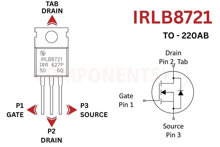
IRLB8721 Pinout Configuration
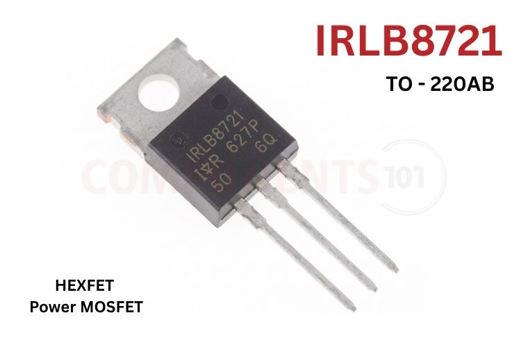
The IRLB8721 is a 30 V, 62 A logic-level N-channel HEXFET power MOSFET in a TO-220AB package.The IRLB8721 is supplied in the industry-standard 3-pin through-hole TO-220AB package. The pin assignments and terminal functions are summarised below:
| Pin Number | Pin Name | Terminal Type | Functional Description |
| 1 | Gate (G) | Control Terminal | Logic-level gate control terminal. Voltage applied relative to Source turns the MOSFET channel ON or OFF. |
| 2 / Tab | Drain (D) | High-Current Channel | Main switching terminal connected to the low-side of the load. Internally shorted to the metal mounting tab. |
| 3 | Source (S) | High-Current Return | Return terminal connected directly to circuit ground (0V) or current sense resistor. |
*Note: The metal mounting tab of the TO-220AB package is internally bonded to Pin 2 (Drain). When mounting the device onto an external metal heatsink, an insulating thermal pad (silicone/mica) and isolating bushing must be used if the heatsink is tied to chassis or circuit ground.
IRLB8721 Package & Ordering Information
The IRLB8721 is available in lead-free / RoHS-compliant packaging denoted by the PbF suffix:
| Part Number | Package Type | Mounting Style | Lead Finish | Thermal Resistance (RθJC) | Ordering / Tape Code |
| IRLB8721PbF | TO-220AB | Leaded Through-Hole | 100% Matte Tin (Pb-Free) | 2.3°C/W (Junction-to-Case) | Bulk Tube (50 Units / Tube) |
*Note: The marking on the front plastic body typically reads "IRLB8721" with a date code, assembly site identifier, and a "P" designating lead-free manufacturing.
IRLB8721 Key Features & Specifications
- Transistor Polarity & Type: N-Channel Logic-Level HEXFET Power MOSFET
- Drain-to-Source Breakdown Voltage (VDS / V(BR)DSS): 30V min (at VGS = 0V, ID = 250 µA)
- Gate-to-Source Voltage (VGS): ±20V max
- Continuous Drain Current (ID): 62 A at TC = 25°C, VGS = 10V (44 A at TC = 100°C)
- Pulsed Drain Current (IDM): 250 A (pulse width limited by maximum Tj)
- Static Drain-Source On-Resistance (RDS(on)) at 10V: 6.5 mΩ typ, 8.7 mΩ max (at VGS = 10V, ID = 31A)
- Static Drain-Source On-Resistance (RDS(on)) at 4.5V: 13.1 mΩ typ, 16.0 mΩ max (at VGS = 4.5V, ID = 25A)
- Gate Threshold Voltage (VGS(th)): 1.35V min, 1.80V typ, 2.35V max (at VDS = VGS, ID = 25 µA)
- Total Gate Charge (Qg): 7.6 nC typ, 13 nC max (at VDS = 15V, VGS = 4.5V, ID = 25A)
- Gate-to-Drain (Miller) Charge (Qgd): 3.4 nC typ
- Input Capacitance (Ciss): 1077 pF typ (at VDS = 15V, VGS = 0V, f = 1.0 MHz)
- Output Capacitance (Coss): 360 pF typ
- Reverse Transfer Capacitance (Crss): 110 pF typ
- Operating Junction & Storage Temperature: -55°C to +175°C
*Note: Complete Technical Details can be found in the IRLB8721 datasheet given at the end of this page.
IRLB8721 Equivalent & Alternative Components
| Equivalent Part | Max VDS | Max ID | Max RDS(on) (Logic) | Package | Key Features & Applications |
| IRLZ44N | 55V | 47A | 22 mΩ (at VGS = 5.0V) | TO-220AB | Classic logic-level power MOSFET; higher voltage rating (55V) but slightly higher RDS(on). |
| FQP30N06L | 60V | 32A | 35 mΩ (at VGS = 5.0V) | TO-220 | 60V logic-level standard; widely used in 24V DC motors and industrial switching. |
| STP55NF06L | 60V | 55A | 18 mΩ (at VGS = 5.0V) | TO-220 | High-current logic-level power switch with rugged avalanche energy rating. |
| IRLB3034 | 40V | 195A | 1.7 mΩ (at VGS = 4.5V) | TO-220AB | Ultra-low resistance powerhouse for heavy 50A+ loads and electric vehicle ESCs. |
| AO3400A | 30V | 5.7A | 33 mΩ (at VGS = 4.5V) | SOT-23 | Miniature logic-level SMD alternative for compact sub-5A PCB load switching. |
What Is the IRLB8721 MOSFET?
The IRLB8721 MOSFET belongs to International Rectifier's logic-level family of power MOSFETs, specifically engineered to eliminate the performance gap between low-voltage digital microcontrollers and high-power DC loads.
In conventional power MOSFETs (such as the ubiquitous IRFZ44N or IRF540N), the gate threshold voltage VGS(th) ranges between 2.0V and 4.0V, with full channel saturation requiring a gate drive of VGS = 10V. When a hobbyist or engineer attempts to drive a standard MOSFET directly from a 5V Arduino or 3.3V ESP32 GPIO pin, the transistor operates in its partially-conductive linear region. Under this condition, the effective channel resistance skyrockets from milliohms to several ohms. At load currents above 2A to 3A, this causes severe I²R resistive heating, leading to catastrophic thermal runaway and transistor destruction.
The IRLB8721 solves this issue fundamentally through tailored gate oxide thickness and channel doping. Its gate threshold voltage is lowered to VGS(th) = 1.35V to 2.35V, and its conduction channel achieves near-complete saturation at just VGS = 4.5V (RDS(on) ≤ 16 mΩ, typ. 13.1 mΩ). Even when driven directly from a 3.3V microcontroller (such as an ESP32, STM32, or Raspberry Pi Pico), the channel resistance remains low (approximately 16 mΩ to 20 mΩ).
At 0.40 W, the TO-220AB package easily dissipates the heat directly into ambient air without requiring an external heatsink. Furthermore, the IRLB8721 features an ultra-low total gate charge of Qg = 7.6 nC. Because microcontroller GPIO pins have strict current limits (typically 20 mA to 40 mA), a lower gate charge means the gate capacitance charges and discharges rapidly, enabling clean, high-frequency pulse-width modulation (PWM) up to 20 kHz to 50 kHz without overheating the microcontroller's internal output drivers.
IRLB8721 Datasheet
Download the official manufacturer IRLB8721 Datasheet for the IRLB8721 N-Channel Logic-Level Power MOSFET. It contains the absolute maximum ratings, RDS(on) versus gate voltage curves, gate-charge and capacitance data, safe operating area, thermal data and the TO-220AB outline drawing.
IRLB8721 Circuit Diagram: How to Use It as a Low-Side Switch
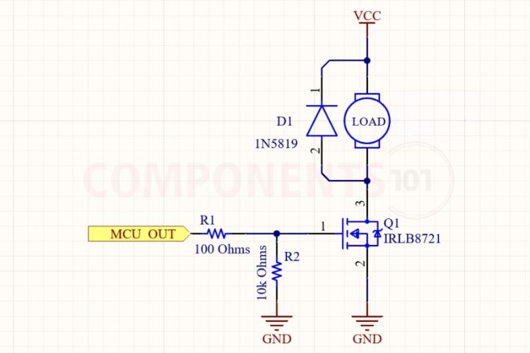
The IRLB8721 is most commonly deployed in a low-side DC load switch configuration to regulate high-power 12V or 24V devices (such as brushed DC motors, LED strips, solenoids, and heating elements) directly from microcontroller GPIO pins.
Circuit Operation & Component Selection
The IRLB8721 MOSFET interfaces with a 3.3V or 5V microcontroller GPIO through a 100 Ω gate resistor (RG) to limit charging current and reduce ringing. A 10 kΩ gate-to-source pull-down resistor (RGS) keeps the MOSFET OFF during startup or reset. In low-side switching, the load connects between +12V and the Drain, while the Source connects to ground. A LOW GPIO signal turns the MOSFET OFF, whereas a HIGH signal turns it ON, providing low-resistance switching with minimal voltage drop. For inductive loads, a reverse-parallel flyback diode (1N5819 or 1N4007) suppresses back-EMF spikes, while a 100 µF, 25V bulk capacitor across the supply rails helps reduce power-supply ripple during switching.
IRLB8721 Applications
- DC Motor Speed Control & PWM Drivers: High-frequency low-side switching for 12V and 24V brushed DC motors in robotics, power tools, and automated actuators.
- High-Power LED Strip Dimming: Flicker-free PWM dimming for 12V/24V architectural, automotive, and aquarium LED strips without requiring large heatsinks.
- Solenoid & Relay Actuation: Fast, spark-free driving of automotive fuel injectors, pneumatic solenoid valves, and electromagnetic door latches.
- 3D Printer Heated Beds & Extruders: Direct logic-level heater control in RepRap and Marlin 3D printers directly from ATmega2560 or STM32 controller boards.
- Synchronous Buck Regulators: High-side and low-side switching in step-down DC-DC converters for telecommunications and server motherboards.
- Solid-State Battery Disconnect Switches: Low-loss electronic circuit breakers and reverse polarity protection in portable battery-powered electronics.
IRLB8721 2D Model and Component Dimensions
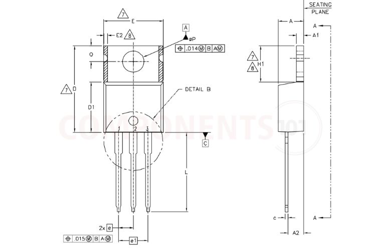
For PCB layout engineers and CAD designers designing custom footprints in KiCad, Altium Designer, Eagle, or EasyEDA, the mechanical dimensions for the standard TO-220AB through-hole package are detailed below:
| Dimension Parameter | Symbol | Min (mm) | Typ (mm) | Max (mm) | Min (Inches) | Max (Inches) |
| Package Body Thickness | A | 3.56 | 4.57 | 4.83 | 0.140 | .0.190 |
| Lead Width | b | 0.38 | 0.81 | 1.02 | 0.015 | 0.040 |
| Lead Shoulder Width | b1 | 1.14 | 1.27 | 1.78 | 0.045 | 0.070 |
| Lead Thickness | c | 0.36 | 0.46 | 0.61 | 0.014 | 0.024 |
| Total Body Height | D | 14.22 | 15.87 | 16.51 | 0.560 | 0.650 |
| Mounting Tab Height | D1 | 8.38 | 8.64 | 9.02 | 0.330 | 0.355 |
| Package Body Width | E | 9.65 | 10.16 | 10.67 | 0.380 | 0.420 |
| Lead Pitch (Pin-to-Pin) | e | - | 2.54 | - | - | 0.100 |
| Mounting Tab Thickness | H1 | 1.14 | 1.27 | 1.40 | 0.045 | 0.055 |
| Lead Length | L | 12.70 | 13.72 | 14.73 | 0.500 | 0.580 |
| Mounting Hole Diameter | ØP | 3.53 | 3.84 | 4.09 | 0.139 | 0.161 |
| Hole Center to Body Edge | Q | 2.54 | 2.79 | 3.43 | 0.100 | 0.135 |